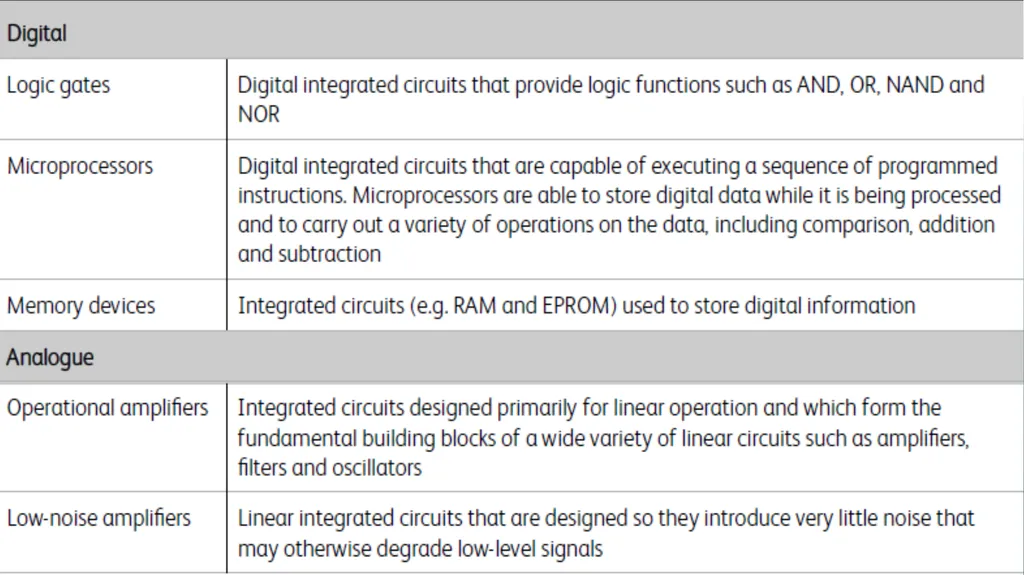
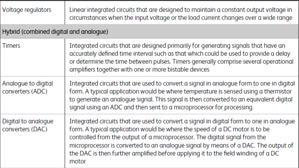
INTEGRATED CIRCUITS SCALE OF INTEGRATION FABRICATION TECHNOLOGY Integrated circuits are fabricated on wafers of very pure silicon. The layers of semiconductor material are fabricated by means of a photographic process using ultraviolet
"INTEGRATED CIRCUITS SCALE OF INTEGRATION" is the property of its rightful owner. Permission is granted to
download and print the materials on this website for personal, non-commercial use only, and to display it
on your personal computer provided you do not modify the materials and that you retain all copyright
notices contained in the materials. By downloading content from our website, you accept the terms of this
agreement.
Presentation Transcript
01
INTEGRATED CIRCUITS<br>
02
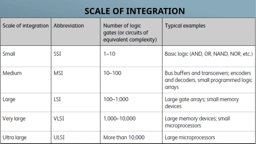
SCALE OF INTEGRATION<br>
03
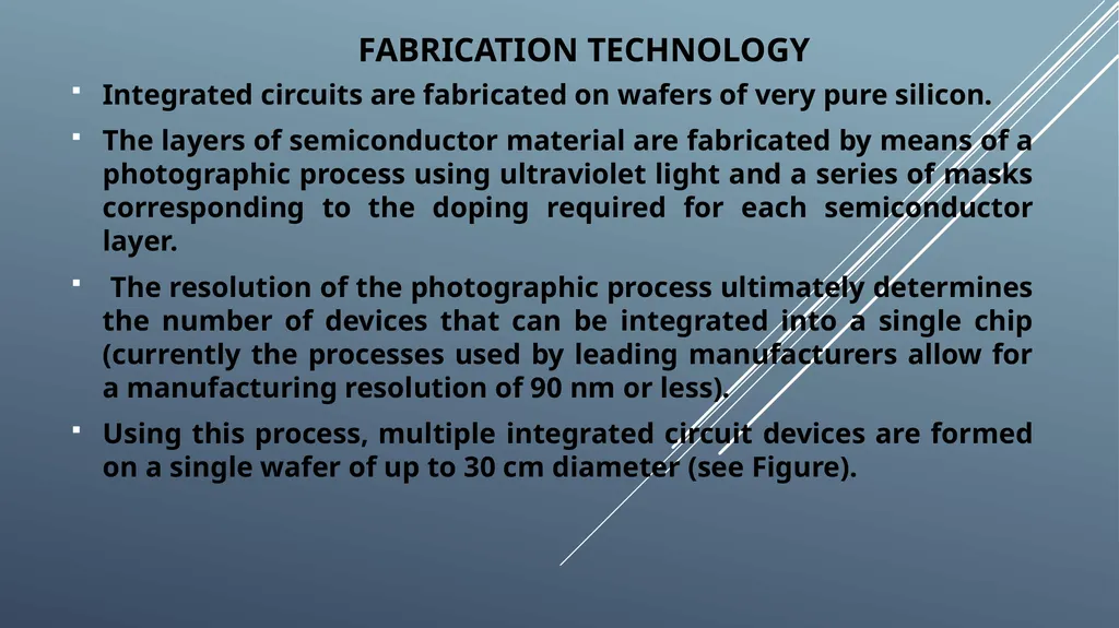
FABRICATION TECHNOLOGY Integrated circuits are fabricated on wafers of very pure silicon.
The layers of semiconductor material are fabricated by means of a photographic process using ultraviolet light and a series of masks corresponding to the doping required for each semiconductor layer.
The resolution of the photographic process ultimately determines the number of devices that can be integrated into a single chip (currently the processes used by leading manufacturers allow for a manufacturing resolution of 90 nm or less).
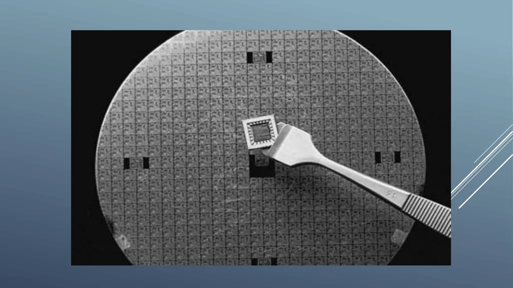
Using this process, multiple integrated circuit devices are formed on a single wafer of up to 30 cm diameter (see Figure).<br>
04
FABRICATION TECHNOLOGY When the doping process is complete, the wafer is tested before being cut into small rectangular areas called dice.
Non-functional die are marked and rejected while those that are functional move on to the next stage of the process, which involves mounting the die into a package using aluminium (or gold) wires which are welded to pads formed around the edge of the die.
These tiny wires form the connection from the die to the connecting or soldering pins on the package in which the die is finally mounted and hermetically sealed.
Testing accounts for a significant proportion of the production cost, and low yield on the more complex devices (VLSI and ULSI packages) can be problematic and, as a result, costs can be high.<br>
05
PACKAGING AND PIN NUMBERING The earliest integrated circuits were packaged in ceramic flat packs.
These were used in military and critical aerospace applications for several decades due to their small size and high reliability.
Packaging of integrated circuits for domestic, consumer and industrial applications moved quickly to the popular dual in-line package (DIL or DIP).
The first generation of DIL integrated circuits were supplied in ceramic packages, but lower-cost plastic packages quickly became popular for non-critical applications, such as the first generation of personal computers.
With the advent of powerful 16- and 32-bit microprocessors, pin counts of VLSI circuits exceeded the practical limit for DIP packaging (around 68 pins) and so the pin grid array (PGA) and leadless chip carrier (LCC) or plastic leadless chip carrier (PLCC) packages were introduced.<br>
06
PACKAGING AND PIN NUMBERING Surface-mounted integrated circuits used connections that were more closely spaced, with their connections formed as either gull-wing or J-lead, as exemplified by the small-outline integrated circuit (SOIC).
PGA packages are still in common use but, PQFP and TSOP packages were introduced as a more space-efficient solution for integrated circuits with a high pin count (several hundred pins, or more).
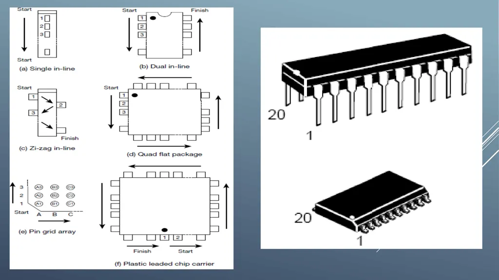
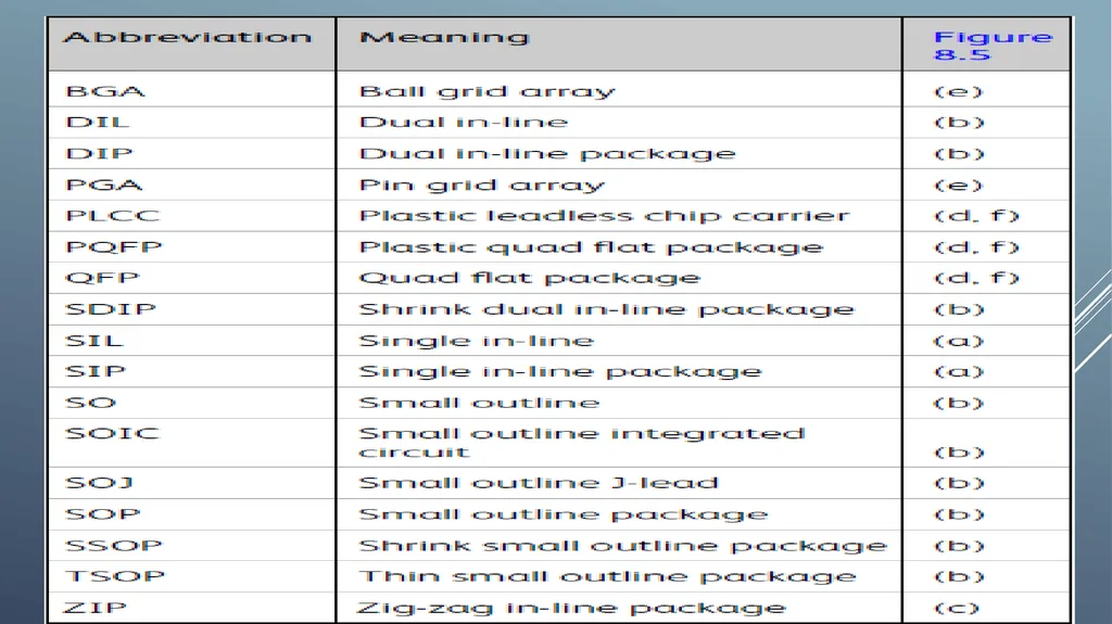
Table below summarizes the various types of integrated circuit package; Figure 1 shows the corresponding pin numbering schemes. These are shown looking from the top of the device.
It is important to note that manufacturers often provide differently packaged versions of the same integrated circuit device.
The different variants are usually distinguished by additional letters and/or numbers in the device coding. Figure 2 shows an example of two different styles of packaging used for a small MSI device.<br>