
Solid state physics Lecture (11) Characterization

Description: Solid state physics Lecture (11) Characterization equipment Prof. Dr. Wisam J. Aziz إ Characterization equipment Characterization, when used in materials science, refers to the broad and general process by which a materials structure and
Related Topics
Download Presentation
"Solid state physics Lecture (11) Characterization" is the property of its rightful owner. Permission is granted to download and print the materials on this website for personal, non-commercial use only, and to display it on your personal computer provided you do not modify the materials and that you retain all copyright notices contained in the materials. By downloading content from our website, you accept the terms of this agreement.
Presentation Transcript
slide1. Solid state physics
Lecture (11)
Characterization equipment
Prof. Dr. Wisam J. Aziz
إ<br>
slide2. Characterization equipment Characterization, when used in materials science, refers to the broad and general process by which a material's structure and properties are probed and measured. It is a fundamental process in the field of materials science, without which no scientific understanding of engineering materials could be ascertained.<br>
slide3. Optical microscope The optical microscope, also referred to as a light microscope, is a type of microscope that commonly uses visible light and a system of lenses to generate magnified images of small objects. Optical microscopes are the oldest design of microscope and were possibly invented in their present compound form in the 17th century. Basic optical microscopes can be very simple, although many complex designs aim to improve resolution and sample contrast<br>
slide4. The object is placed on a stage and may be directly viewed through one or two eyepieces on the microscope. In high-power microscopes, both eyepieces typically show the same image, but with a stereo microscope, slightly different images are used to create a 3-D effect. A camera is typically used to capture the image (micrograph).<br>
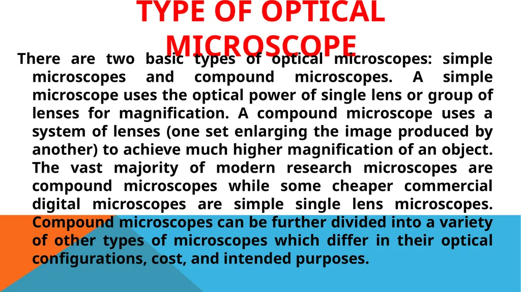
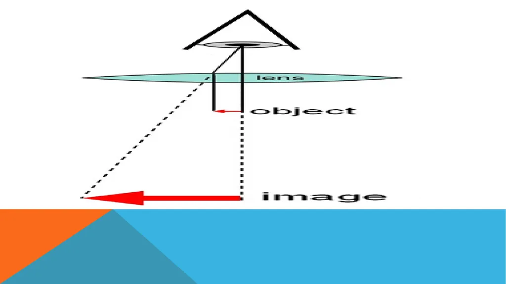
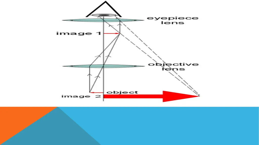
slide5. Type of optical microscope There are two basic types of optical microscopes: simple microscopes and compound microscopes. A simple microscope uses the optical power of single lens or group of lenses for magnification. A compound microscope uses a system of lenses (one set enlarging the image produced by another) to achieve much higher magnification of an object. The vast majority of modern research microscopes are compound microscopes while some cheaper commercial digital microscopes are simple single lens microscopes. Compound microscopes can be further divided into a variety of other types of microscopes which differ in their optical configurations, cost, and intended purposes.<br>
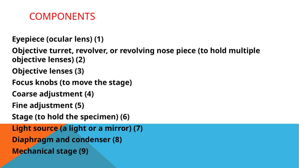
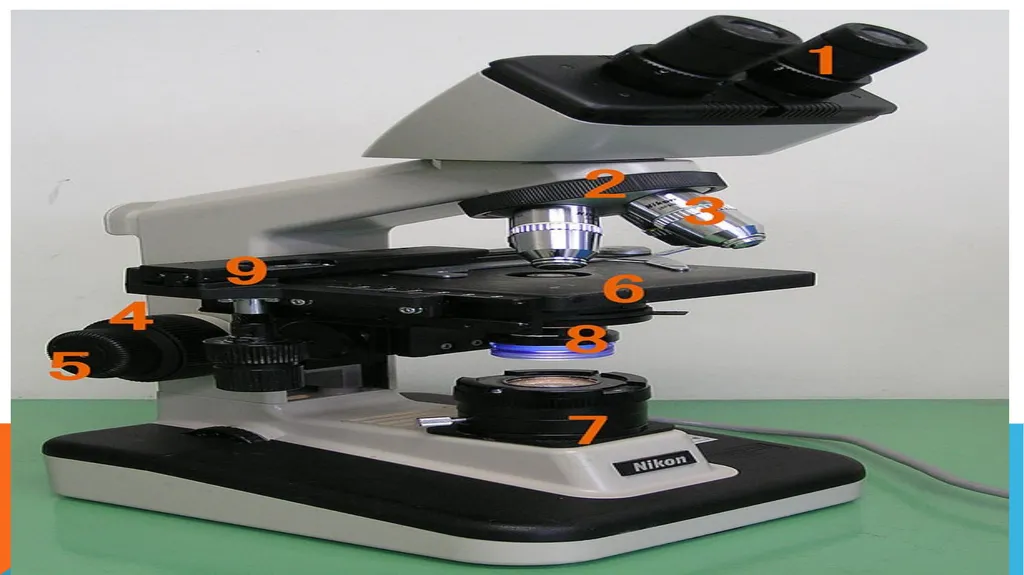
slide8. components Eyepiece (ocular lens) (1)
Objective turret, revolver, or revolving nose piece (to hold multiple objective lenses) (2)
Objective lenses (3)
Focus knobs (to move the stage)
Coarse adjustment (4)
Fine adjustment (5)
Stage (to hold the specimen) (6)
Light source (a light or a mirror) (7)
Diaphragm and condenser (8)
Mechanical stage (9)<br>
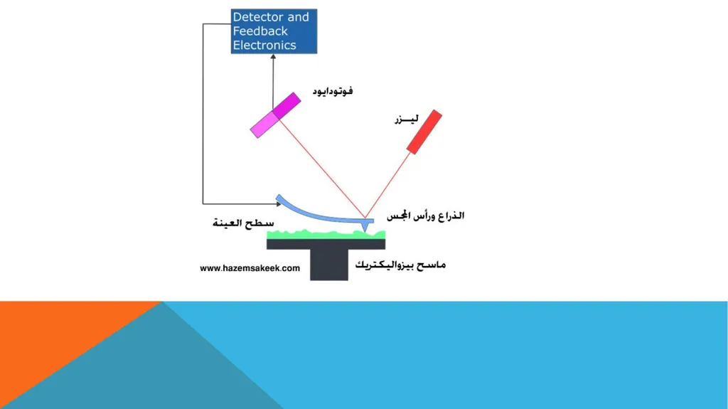
slide10. AFM Atomic force microscopy (AFM) is an influential surface analysis technique used for micro/nanostructured coatings. This flexible technique can be used to obtain high-resolution nanoscale images and study local sites in air (conventional AFM) or liquid (electrochemical AFM) surroundings<br>
slide11. The principle of operation of the device The device consists of a needle with micron dimensions that passes over the surface to be scanned, this needle is fixed to a horizontal holder while it is itself perpendicular to this holder and on the surface to be scanned, a laser beam is projected onto the holder, which rises and falls with the height and fall of the needle, and thus with a variety Surface topography from high and low, and the laser beam reflex is captured on the holder on a receiver. Thus the topography of the scanned surface is determined and drawn according to the movement of the laser beam reflex<br>
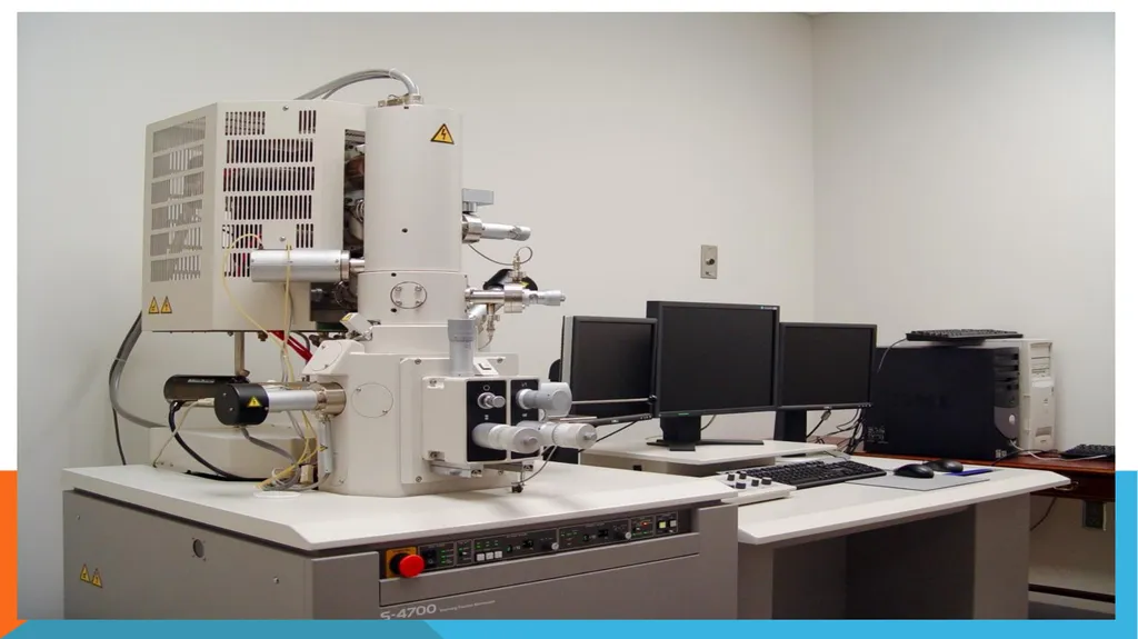
slide13. Field emission scanning electron microscopy (FESEM) Field emission scanning electron microscopy (FESEM) provides topographical and elemental information at magnifications of 10x to 300,000x, with virtually unlimited depth of field. Compared with convention scanning electron microscopy (SEM), field emission SEM (FESEM) produces clearer, less electrostatically distorted images with spatial resolution down to 1 1/2 nanometers – three to six times better.<br>
slide14. Other advantages of FESEM include: The ability to examine smaller-area contamination spots at electron accelerating voltages compatible with energy dispersive spectroscopy (EDS).
Reduced penetration of low-kinetic-energy electrons probes closer to the immediate material surface.
High-quality, low-voltage images with negligible electrical charging of samples (accelerating voltages ranging from 0.5 to 30 kilovolts).
Essentially no need for placing conducting coatings on insulating materials.<br>
slide15. Applications: Applications of FESEM include: Semiconductor device cross section analyses for gate widths, gate oxides, film thicknesses, and construction details
Advanced coating thickness and structure uniformity determination
Small contamination feature geometry and elemental composition measurement<br>
slide16. Principle of Operation A field-emission cathode in the electron gun of a scanning electron microscope provides narrower probing beams at low as well as high electron energy, resulting in both improved spatial resolution and minimized sample charging and damage. For applications that demand the highest magnification possible, we also offer in-lens FESEM.<br>
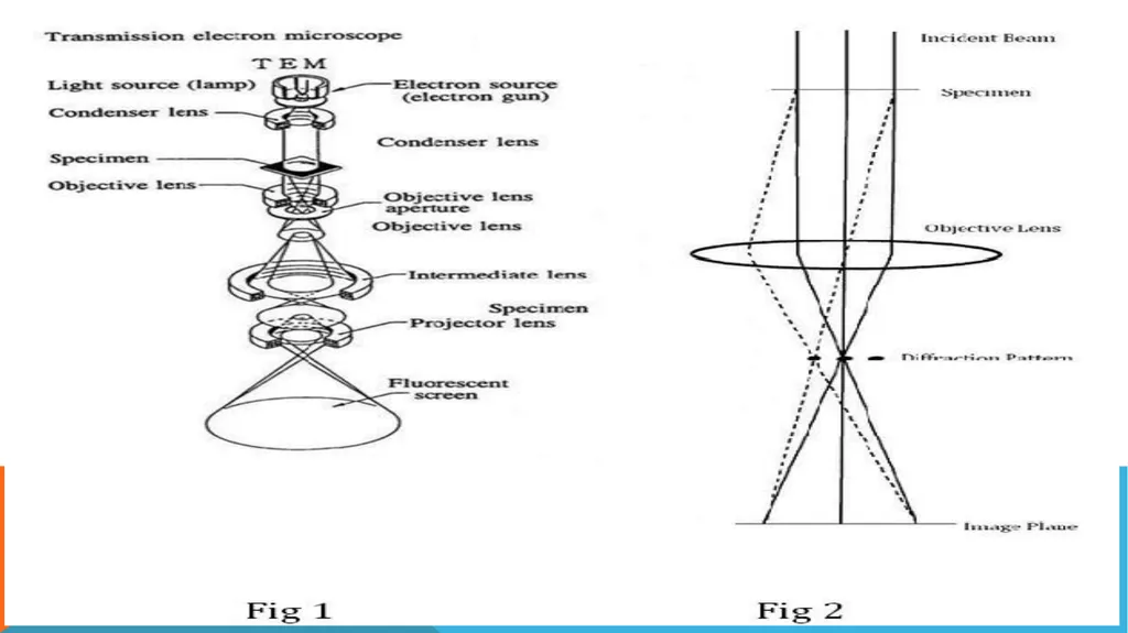
slide18. Transmission Electron Microscopy (TEM) The transmission electron microscope is a very powerful tool for material science. A high energy beam of electrons is shone through a very thin sample, and the interactions between the electrons and the atoms can be used to observe features such as the crystal structure and features in the structure like dislocations and grain boundaries. Chemical analysis can also be performed. TEM can be used to study the growth of layers, their composition and defects in semiconductors. High resolution can be used to analyze the quality, shape, size and density of quantum wells, wires and dots.<br>
slide19. Transmission Electron Microscopy (TEM) The TEM operates on the same basic principles as the light microscope but uses electrons instead of light. Because the wavelength of electrons is much smaller than that of light, the optimal resolution attainable for TEM images is many orders of magnitude better than that from a light microscope. Thus, TEMs can reveal the finest details of internal structure - in some cases as small as individual atoms.<br>
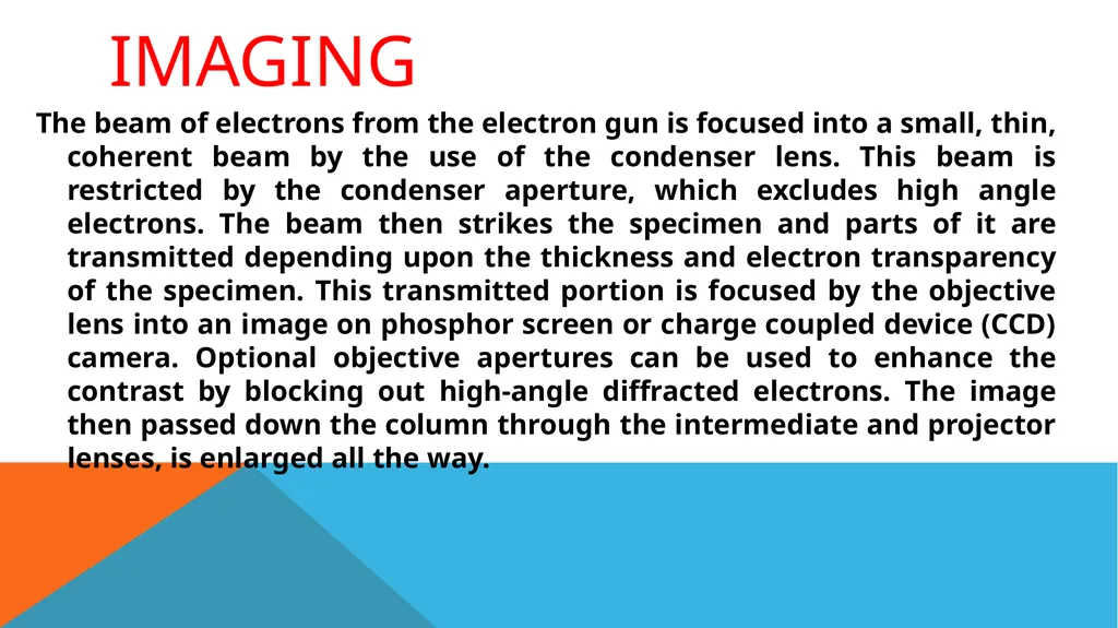
slide21. Imaging The beam of electrons from the electron gun is focused into a small, thin, coherent beam by the use of the condenser lens. This beam is restricted by the condenser aperture, which excludes high angle electrons. The beam then strikes the specimen and parts of it are transmitted depending upon the thickness and electron transparency of the specimen. This transmitted portion is focused by the objective lens into an image on phosphor screen or charge coupled device (CCD) camera. Optional objective apertures can be used to enhance the contrast by blocking out high-angle diffracted electrons. The image then passed down the column through the intermediate and projector lenses, is enlarged all the way.<br>
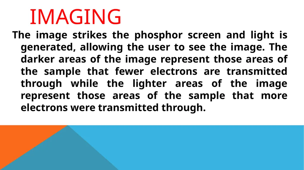
slide22. Imaging The image strikes the phosphor screen and light is generated, allowing the user to see the image. The darker areas of the image represent those areas of the sample that fewer electrons are transmitted through while the lighter areas of the image represent those areas of the sample that more electrons were transmitted through.<br>
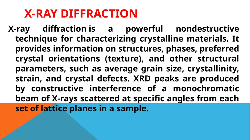
slide23. X-ray diffraction X-ray diffraction is a powerful nondestructive technique for characterizing crystalline materials. It provides information on structures, phases, preferred crystal orientations (texture), and other structural parameters, such as average grain size, crystallinity, strain, and crystal defects. XRD peaks are produced by constructive interference of a monochromatic beam of X-rays scattered at specific angles from each set of lattice planes in a sample.<br>
slide24. X-ray diffraction The peak intensities are determined by the atomic positions within the lattice planes. Consequently, the XRD pattern is the fingerprint of periodic atomic arrangements in a given material. An online search of a standard database for X-ray powder diffraction patterns enables quick phase identification for a large variety of crystalline samples<br>
slide25. Thank you<br>
Lecture (11)
Characterization equipment
Prof. Dr. Wisam J. Aziz
إ<br>
slide2. Characterization equipment Characterization, when used in materials science, refers to the broad and general process by which a material's structure and properties are probed and measured. It is a fundamental process in the field of materials science, without which no scientific understanding of engineering materials could be ascertained.<br>
slide3. Optical microscope The optical microscope, also referred to as a light microscope, is a type of microscope that commonly uses visible light and a system of lenses to generate magnified images of small objects. Optical microscopes are the oldest design of microscope and were possibly invented in their present compound form in the 17th century. Basic optical microscopes can be very simple, although many complex designs aim to improve resolution and sample contrast<br>
slide4. The object is placed on a stage and may be directly viewed through one or two eyepieces on the microscope. In high-power microscopes, both eyepieces typically show the same image, but with a stereo microscope, slightly different images are used to create a 3-D effect. A camera is typically used to capture the image (micrograph).<br>
slide5. Type of optical microscope There are two basic types of optical microscopes: simple microscopes and compound microscopes. A simple microscope uses the optical power of single lens or group of lenses for magnification. A compound microscope uses a system of lenses (one set enlarging the image produced by another) to achieve much higher magnification of an object. The vast majority of modern research microscopes are compound microscopes while some cheaper commercial digital microscopes are simple single lens microscopes. Compound microscopes can be further divided into a variety of other types of microscopes which differ in their optical configurations, cost, and intended purposes.<br>
slide8. components Eyepiece (ocular lens) (1)
Objective turret, revolver, or revolving nose piece (to hold multiple objective lenses) (2)
Objective lenses (3)
Focus knobs (to move the stage)
Coarse adjustment (4)
Fine adjustment (5)
Stage (to hold the specimen) (6)
Light source (a light or a mirror) (7)
Diaphragm and condenser (8)
Mechanical stage (9)<br>
slide10. AFM Atomic force microscopy (AFM) is an influential surface analysis technique used for micro/nanostructured coatings. This flexible technique can be used to obtain high-resolution nanoscale images and study local sites in air (conventional AFM) or liquid (electrochemical AFM) surroundings<br>
slide11. The principle of operation of the device The device consists of a needle with micron dimensions that passes over the surface to be scanned, this needle is fixed to a horizontal holder while it is itself perpendicular to this holder and on the surface to be scanned, a laser beam is projected onto the holder, which rises and falls with the height and fall of the needle, and thus with a variety Surface topography from high and low, and the laser beam reflex is captured on the holder on a receiver. Thus the topography of the scanned surface is determined and drawn according to the movement of the laser beam reflex<br>
slide13. Field emission scanning electron microscopy (FESEM) Field emission scanning electron microscopy (FESEM) provides topographical and elemental information at magnifications of 10x to 300,000x, with virtually unlimited depth of field. Compared with convention scanning electron microscopy (SEM), field emission SEM (FESEM) produces clearer, less electrostatically distorted images with spatial resolution down to 1 1/2 nanometers – three to six times better.<br>
slide14. Other advantages of FESEM include: The ability to examine smaller-area contamination spots at electron accelerating voltages compatible with energy dispersive spectroscopy (EDS).
Reduced penetration of low-kinetic-energy electrons probes closer to the immediate material surface.
High-quality, low-voltage images with negligible electrical charging of samples (accelerating voltages ranging from 0.5 to 30 kilovolts).
Essentially no need for placing conducting coatings on insulating materials.<br>
slide15. Applications: Applications of FESEM include: Semiconductor device cross section analyses for gate widths, gate oxides, film thicknesses, and construction details
Advanced coating thickness and structure uniformity determination
Small contamination feature geometry and elemental composition measurement<br>
slide16. Principle of Operation A field-emission cathode in the electron gun of a scanning electron microscope provides narrower probing beams at low as well as high electron energy, resulting in both improved spatial resolution and minimized sample charging and damage. For applications that demand the highest magnification possible, we also offer in-lens FESEM.<br>
slide18. Transmission Electron Microscopy (TEM) The transmission electron microscope is a very powerful tool for material science. A high energy beam of electrons is shone through a very thin sample, and the interactions between the electrons and the atoms can be used to observe features such as the crystal structure and features in the structure like dislocations and grain boundaries. Chemical analysis can also be performed. TEM can be used to study the growth of layers, their composition and defects in semiconductors. High resolution can be used to analyze the quality, shape, size and density of quantum wells, wires and dots.<br>
slide19. Transmission Electron Microscopy (TEM) The TEM operates on the same basic principles as the light microscope but uses electrons instead of light. Because the wavelength of electrons is much smaller than that of light, the optimal resolution attainable for TEM images is many orders of magnitude better than that from a light microscope. Thus, TEMs can reveal the finest details of internal structure - in some cases as small as individual atoms.<br>
slide21. Imaging The beam of electrons from the electron gun is focused into a small, thin, coherent beam by the use of the condenser lens. This beam is restricted by the condenser aperture, which excludes high angle electrons. The beam then strikes the specimen and parts of it are transmitted depending upon the thickness and electron transparency of the specimen. This transmitted portion is focused by the objective lens into an image on phosphor screen or charge coupled device (CCD) camera. Optional objective apertures can be used to enhance the contrast by blocking out high-angle diffracted electrons. The image then passed down the column through the intermediate and projector lenses, is enlarged all the way.<br>
slide22. Imaging The image strikes the phosphor screen and light is generated, allowing the user to see the image. The darker areas of the image represent those areas of the sample that fewer electrons are transmitted through while the lighter areas of the image represent those areas of the sample that more electrons were transmitted through.<br>
slide23. X-ray diffraction X-ray diffraction is a powerful nondestructive technique for characterizing crystalline materials. It provides information on structures, phases, preferred crystal orientations (texture), and other structural parameters, such as average grain size, crystallinity, strain, and crystal defects. XRD peaks are produced by constructive interference of a monochromatic beam of X-rays scattered at specific angles from each set of lattice planes in a sample.<br>
slide24. X-ray diffraction The peak intensities are determined by the atomic positions within the lattice planes. Consequently, the XRD pattern is the fingerprint of periodic atomic arrangements in a given material. An online search of a standard database for X-ray powder diffraction patterns enables quick phase identification for a large variety of crystalline samples<br>
slide25. Thank you<br>