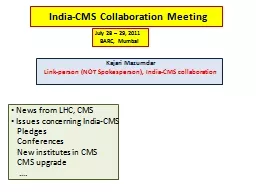
ABhardwaj AKumar M Naimuddin KRanjan RKShivpuri Center for Detector amp Related Software Technology CDRST Delhi University DU Delhi India IndiaCMS Meeting BARC 28 July 29 July 2011 ID: 450042
Download Presentation The PPT/PDF document "DU’s proposed participation in the CMS..." is the property of its rightful owner. Permission is granted to download and print the materials on this web site for personal, non-commercial use only, and to display it on your personal computer provided you do not modify the materials and that you retain all copyright notices contained in the materials. By downloading content from our website, you accept the terms of this agreement.
Slide1
DU’s proposed participation in the CMS Upgrade – Phase-II R&D
A.Bhardwaj, A.Kumar, M. Naimuddin, K.Ranjan, R.K.ShivpuriCenter for Detector & Related Software Technology (CDRST) Delhi University (DU), Delhi, India
India-CMS Meeting,
BARC, 28 July – 29 July, 2011Slide2
Si Tracker Upgrade
Ashutosh Bhardwaj, Kirti Ranjan, R.K. ShivpuriSlide3
Our Interest
Showed interest in Si Upgrade in Tracker in 2010Discussed with Frank Hartmann (then coordinating the overall sensor R&D activities and now Deputy PM) & Duccio Abbaneo (phase 2 overall coordination incharge) in May 2010. Several approved R&D projects for phase-II. Phase I R&D was frozen. “Development of pixel and micro-strip sensors on radiation tolerant substrates for the tracker upgrade at SLHC”: Contact Person: M. de Palma ; submitted: April 2008 ; status: Approved; CMS SLHC RD #08.03 “Materials, technologies and simulations for silicon sensor modules at intermediate to large radii of a new CMS tracker for SLHC” ; Hamburg, Karlsruhe, Louvain, Vienna, Vilnius; submitted: March 2008 ; status: Approved; CMS SLHC RD # 08.02
As a first step, we mutually decided to start up with some effort at DU in the existing R&D and then put up a formal presentation in the Tracker
Group => Si Device SimulationSlide4
Proposal from
Frank Hartmann on Si Device Simulation (July 2010): The 12 strip of the multi-geometry strip cells, which comes withdifferent pitches & widths, in p-in-n & n-in-n version, also withp-spray and p-stop (isolation)The first goal should be to understand (interstrip)
capacitance values, isolation and breakdown to support the measurements
we are going to do.
Further steps could be possible improvements of the geometry.
Understanding of behavior after irradiation
.
As a second step, we should simulate some cells of the multi-geometrylong pixel structures, which come in the same configuration but inaddition with Rpoly biasing & punch-through biasing…
Si Device Simulation
Alberto
Messino
(Upgrade Sensor WG convener)
volunteered to step in to define and watch the simulation program.
Start with a sort of "calibration" or better a
comparison of our simulation with existing published work.
Claudio
Piemonte
,
Device Simulations of Isolation Techniques for Silicon
Microstrip
Detectors Made on p-Type
Substrates,
in
«IEEE TRANSACTIONS ON NUCLEAR
SCIENCE»,vol
. 53,n. 3,
2006
, pp. 1694-1705Slide5
http://cms-tracker.web.cern.ch/cms-tracker/TKorganisation/Phase2_Organization-DA.pdf
Tracker – Phase 2 OrganizationSlide6
Si Device Simulation– First Results
Tracker Week Meetings (11 - 15 Oct. 2010, CERN)https://indico.cern.ch/conferenceDisplay.py?confId=80952 - Upgrade Sensor WG meeting, -
Frank Hartman (Sensor Technology Co-ordinator)
https://
indico.cern.ch/getFile.py/access?contribId=0&sessionId=3&resId=1&materialId=slides&confId=80952Slide7
Si Device Simulation– First Results
Simulation effort to support the HPK campaign 20‘https://indico.cern.ch/getFile.py/access?contribId=2&sessionId=3&resId=1&materialId=slides&confId=80952Device Simulation Using ATLAS- Device Simulation Program From SilvacoTwo n+ neighbouring strips, with two intermediate p+ stops.
Report to Collaboration in India-CMS Meeting, 28 Oct. – 29 Oct. 2010 Slide8
Si Device Simulation– First Results
Upgrade Plenary Meeting; Friday 15 October 2010Progress and plans for sensors R&D 20' Speaker: F. HartmannSlide9
Si Device Simulation– Further work
Continuous EVO meetings and discussions with Alberto MessinoPresented Results on MSSD Simulation in Tracker Week Meetings, 14 - 18 Feb. 2011 https://indico.cern.ch/conferenceDisplay.py?confId=125774MSSD Simulation Results 20'
https://indico.cern.ch/getFile.py/access?contribId=1&resId=0&materialId=slides&confId=125774Slide10
Si Device Simulation– Further work
Comparison Experimental/Simulation MeasurementDesign # 3
At low voltage the dip in the capacitance is similar
At Saturation, Exp DC-
Cint
= 0.9 pF
>
Sim DC-Cint = 0.63pF
Exp Vsaturation = 200-250V >
Sim
Vsaturation
= 100-150V
0.9pF
0.63 pF
200-250V
100-150V
Similar behavior for low voltage
10
EXP
Cint
SIM DC
Cint
Q
F
= 1e10 cm
-2 Slide11
Upgrade Phase II Plenary, 14 Feb. - 18 Feb. 2011
Overview of HPK sensors project, Alexander Dierlamm 45' https://indico.cern.ch/getFile.py/access?contribId=1&resId=1&materialId=slides&confId=127280Si Device Simulation– Further workSlide12
Several groups showed their interests in Process/Device Simulation
Si Device Simulation– Further workSlide13
Simulation – SLHC Sensor R&D
https://twiki.cern.ch/twiki/bin/viewauth/CMS/SLHCSensorDevelopmenthttps://twiki.cern.ch/twiki/bin/viewauth/CMS/SLHCSensorDevelopment#Simulationshttps://twiki.cern.ch/twiki/pub/CMS/SLHCSensorDevelopment/Simulation_tasks_V1.pdfSlide14
Simulations: Alberto Messineo (Universita di Pisa-Sezione di Pisa (INFN)),
Tracker Week Meetings, 18 – 22 July, 2011 https://indico.cern.ch/getFile.py/access?contribId=8&resId=0&materialId=slides&confId=144303Simulation – SLHC Sensor R&D Slide15
Present Facilities at DU
Ashutosh Bhardwaj, D. U. Class 10000 lab with class 100/1000 laminar flow tables (minor maintenance required)Keithley 237, Keithley 2410, Keithley 590 CV systemCascade Semi-automatic Probe StationKeithley 2400 Semiconductor Characterization System
Few test structures from Frank for characterizationSlide16
Tracker DPG Tasks (service work)
Tracker Alignment using cosmics - present Results on Tracker Alignment inTracker Detector Performance Group Weekly meetings (Thursday 23 June 2011) https://indico.cern.ch/conferenceDisplay.py?confId=127125Weekly Tracker DPG meeting (08 July 2011)https://indico.cern.ch/conferenceDisplay.py?confId=127126
Reported by Alignment conveners (
Gero
Flucke
&
Alessio Bonato) in Tracker General Meeting @ CMS Week, June 28th, 2011 https://indico.cern.ch/getFile.py/access?contribId=5&sessionId=0&resId=0&materialId=slides&confId=142604Slide17
Proposal– SLHC Sensor R&D
We have shown interest in participation in all activities related with Si Sensor R&D in phase II of the CMS – Simulation – already shown encouraging results – will continue.Characterization – few test structures to be characterized.Fabrication of sensors/test structures – will explore the possibility Interested in giving a presentation in Tracker Institutional Board meeting for formal induction 6k CHF /PhD/annum will be needed under M&O-B for Tracker from the year 2013. (for year 2012 – it’s 3k CHF per PhD)
Also interested in joining RD50 (Radiation Hard Si Sensors R&D)
– 3K CHF/institute/annum – lot of
E
uropean facilities/expertiseSlide18
MPGD Upgrade
A.Kumar, Md. Naimuddin, R.K. ShivpuriSlide19
GEMs for CMS high eta upgrade(MPGD)
The Physics case of challenging post-TDR scenario where:-300 fb-1 already collected -centre-of-mass energy: 14TeV, lumi 2-3 x 1034cm-2s-1
-events are with nominal or 2 x nominal pile-up
Physics Goals:
Boosted objects with
muon
-decay channels, asymmetry, coupling & spin measurements, fusion processes.
High luminosity physics:=> making a case for a coherent detector system in the true “forward” eta region
- Triple boson production, Z’ factory physics, Exotic with light object decaying to
muons
The
GEM
technology is likely to be a strong candidate for “forward” tracking:
-spatial resolution ~ 100 microns, time resolution < 5ns, detector efficiency > 98%
-precise tracking and fast trigger information simultaneously
-can be designed with sufficiently fine segmentation to cope with high particle fluxes ~
(
1MHz/mm2
)
at LHC
Slide20
GEMs for CMS high eta upgrade(MPGD)Slide21
GEMs for CMS high eta upgrade(MPGD)
==>Possible participationMPGD R&D and fabrication (GEM foils, mechanics, readout circuits etc)Module testing and characterization (using cosmic muons, X-ray test up)DAQ (Fast Electronics, Power supplies, Cables, Gas mixing unit etc)Beam test participation and online analysis at CERNBeam test Data Analysis Detector SimulationPhysics Potential (MC studies)
==> Possibility of putting PhD students.Slide22
Back UPSlide23
Software:
Silvaco Tools23
Device Simulation
ATLAS (2D Silicon Device Simulator)
S-PISCES (2D Silicon Device Simulator)
LUMINOUS (2D Optoelectronic Device Simulator)
BLAZE (2D Device Simulator for Advanced Materials)
Device 3D (3D Device Simulator)
TFT (Amorphous & Polycrystalline Device Simulator)
QUANTUM (3D Simulation Models for Quantum Mechanical Effects)
FERRO (Ferroelectric Field Dependent Permittivity Model)
Process Simulation
ATHENA Framework
S-SUPREM4 (Process Simulator)
MC Implant (Monte-Carlo Implantation Simulator)
ELITE (Physical Etching and Deposition Simulator)
OPTILITH (2D Optical Lithography Simulator)
MC Deposit/ETCH (2D Monte Carlo Deposition & Etch Simulator)