/
POST OFFICE BOX 655303  DALLAS, TEXAS 75265 POST OFFICE BOX 655303  DALLAS, TEXAS 75265

POST OFFICE BOX 655303 DALLAS, TEXAS 75265 - PDF document

alexa-scheidler
alexa-scheidler . @alexa-scheidler
Follow
407 views
Uploaded On 2016-11-08

POST OFFICE BOX 655303 DALLAS, TEXAS 75265 - PPT Presentation

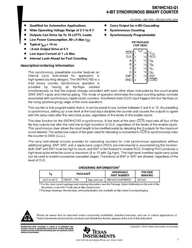
SCLS584A MAY 2004 1 flipflop outputs low after the next lowtohigh transition of CLK regardless of the levels of the enable inputs The carry lookahead circuitry provides for cascading ID: 486420

 SCLS584A MAY 2004

Share:

Link:

Embed:

Download Presentation from below link

Download Pdf The PPT/PDF document "POST OFFICE BOX 655303 DALLAS, TEXAS 75..." is the property of its rightful owner. Permission is granted to download and print the materials on this web site for personal, non-commercial use only, and to display it on your personal computer provided you do not modify the materials and that you retain all copyright notices contained in the materials. By downloading content from our website, you accept the terms of this agreement.


Presentation Transcript

 SCLS584A  MAY 2004  1 POST OFFICE BOX 655303 DALLAS, TEXAS 75265 flip-flop outputs low after the next low-to-high transition of CLK, regardless of the levels of the enable inputs. The carry look-ahead circuitry provides for cascading counters for n-bit synchronous applications withoutadditional gating. ENP, ENT, and a ripple-carry output (RCO) are instrumental in accomplishing this function.can be used to enable successive cascaded stages. Transitions at ENP or ENT are allowed, regardless of theORDERING INFORMATION PACKAGE PART NUMBER TOP-SIDE 40°C Tape and reel HC163I For the most current package and ordering information, see document, or see the TI web site at http://www.ti.com.are available at http://www.ti.com/packaging. Please be aware that an important notice concerning availability, standard warranty, and use in critical applications o f 1234567816151413129CLR CLKACDENPGNDVQAQBQCQDENT Copyright 2008 Texas Instruments Incorporated#*+,( SCLS584A  MAY 2004 POST OFFICE BOX 655303 DALLAS, TEXAS 75265description/ordering information (continued)This counter features a fully independent clock circuit. Changes at control inputs (ENP, ENT, or LOAD operating mode have no effect on the contents of the counter until clocking occurs. The function oflogic diagram (positive logic) 1910731514CLR LOAD For simplicity, routing of complementary signals LD and CK G2G43D4R1 13BQB G2G43D1 12CQC G2G43D1 QD G2G43D4R1 †CK †CKR LD  SCLS584A  MAY 2004  3 POST OFFICE BOX 655303 DALLAS, TEXAS 75265logic symbol, each D/T flip-flop M1 TE (Toggle Enable) CK (Clock) 3D 4R , 2T/1C3D logic diagram, each D/T flip-flop (positive logic) TG CKLDTELD †LD †D R CK †CK †CK †CK The origins of LD and CK are shown in the logic diagram of the overall device. SCLS584A  MAY 2004 POST OFFICE BOX 655303 DALLAS, TEXAS 75265typical clear, preset, count, and inhibit sequence1.Clear outputs to zero (synchronous)2.Preset to binary 123.Count to 13, 14, 15, 0, 1, and 24.Inhibit DataInputsDataOutputsCLR LOAD ABCDCLKENPENTRCOQAQBQCQDAsyncClearSyncClearPreset 1213 1415012  SCLS584A  MAY 2004  5 POST OFFICE BOX 655303 DALLAS, TEXAS 75265absolute maximum ratings over operating free-air temperature range (unless otherwise noted)Supply voltage range, V 0.5 V to 7 V. . . . . . . . . . . . . . . . . . . . . . . . . . . . . . . . . . . . . . . . . . . . . . . . . . . . . . . . . . . . . . . . . . . . . . . . . . . . . . . . . . . . . . . . . . . . . . . . . . . . . . . . . . . . . . . . . . . . . . . . . . . . . . Continuous output current, I. . . . . . . . . . . . . . . . . . . . . . . . . . . . . . . . . . . . . . . . . . . . . . Continuous current through V. . . . . . . . . . . . . . . . . . . . . . . . . . . . . . . . . . . . . . . . . . . . . . . . . . . Package thermal impedance, (see Note 2): PW package 108. . . . . . . . . . . . . . . . . . . . . . . . . . . . . . . . 65. . . . . . . . . . . . . . . . . . . . . . . . . . . . . . . . . . . . . . . . . . . . . . . . . . . Stresses beyond those listed under “absolute maximum ratings” may cause permanent damage to the device. These are stress ratings only, afunctional operation of the device at these or any other conditions beyond those indicated under “recommended operating conditiimplied. Exposure to absolute-maximum-rated conditions for extended periods may affect device reliability.NOTES:1.The input and output voltage ratings may be exceeded if the input and output current ratings are observed.2.The package thermal impedance is calculated in accordance with JESD 51-7.recommended operating conditions (see Note 3) MIN NOM MAX UNIT V Supply voltage 2 5 6 V V V V V V V V V V V V V VI V VO V V t/v‡ ns t/v‡ V ns TA 85 °C NOTE 3:All unused inputs of the device must be held at V or GND to ensure proper device operation. Refer to the TI application report,Implications of Slow or Floating CMOS InputsIf this device is used in the threshold region (from Vgrounding, , functionally,the CLK inputs are not ensured while in the shift, count, or toggle operating modes. SCLS584A  MAY 2004 POST OFFICE BOX 655303 DALLAS, TEXAS 75265electrical characteristics over recommended operating free-air temperature range (unlessotherwise noted) PARAMETER TEST CONDITIONS V TAC MIN MAX UNIT PARAMETER V TYP MAX MIN MAX UNIT 1.998 1.9 I A 4.499 4.4 V V I IL A 5.999 5.9 V V VI or VIL I 4.3 3.84 V I 5.8 5.34 0.1 0.1 I A 0.1 0.1 V V I IL A 0.1 0.1 V V VI or VIL I 0.26 0.33 V I 0.26 0.33 II VI 6 V 0.1 ±100 ±1000 nA I I O 80 µA Ci 10 10 pF timing requirements over recommended operating free-air temperature range (unless otherwise V TAC MIN MAX UNIT V MAX MIN MAX UNIT 5 f clock 25 MHz clock 29 MHz 100 t w Pulse durationCLK high or low 20 ns tw 17 ns 190 38 32 170 LOAD 34 LOAD low 29 215 t ENP, ENT 4.5 V 43 ns t ENP, ENT 37 ns 200 CLR 40 CLR low 34 200 CLR 40 CLR inactive 34 0 t h 0 ns th 0 ns  SCLS584A  MAY 2004  7 POST OFFICE BOX 655303 DALLAS, TEXAS 75265switching characteristics over recommended operating free-air temperature range, C = 50 pF(unless otherwise noted) (see Figure 1) PARAMETER FROM TO V TAC MIN MAX UNIT PARAMETER FROM (INPUT) (OUTPUT) V TYP MAX MIN MAX UNIT 14 5 f 40 25 MHz f 44 29 MHz 215 270 RCO 43 54 CLK RCO 37 46 CLK 205 255 t 41 51 ns t 35 43 ns 195 245 ENT RCO 39 49 ENT RCO 33 42 75 95 t t Any 15 19 ns tt Any 13 16 ns operating characteristics, TPARAMETER TEST CONDITIONS TYP UNIT C pF SCLS584A  MAY 2004 POST OFFICE BOX 655303 DALLAS, TEXAS 75265PARAMETER MEASUREMENT INFORMATIONVOLTAGE WAVEFORMSSETUP AND HOLD AND INPUT RISE AND FALL TIMESVOLTAGE WAVEFORMSPULSE DURATIONS th 90%90% r tfReferenceInputDataInput 50%High-LevelPulse 50% V 50% V VOLTAGE WAVEFORMSPROPAGATION DELAY AND OUTPUT TRANSITION TIMES 90%90% C VO H VO L r tfInputIn-PhaseOutput 50% 50%50%10%10% H VO L trtf NOTES:A.CB.Phase relationships between waveforms were chosen arbitrarily. All input pulses are supplied by generators having the followicharacteristics: PRR C.For clock inputs, fD.The outputs are measured one at a time, with one input transition per measurement.E.t TestUnder TestFigure 1. Load Circuit and Voltage Waveforms  SCLS584A  MAY 2004  9 POST OFFICE BOX 655303 DALLAS, TEXAS 75265APPLICATION INFORMATIONThis application demonstrates how the look-ahead carry circuit can be used to implement a high-speed n-bitcounter. The SN74HC163 counts in binary. Virtually any count mode (modulo-N, NThe application circuit shown in Figure 2 is not valid for clock frequencies above 18 MHz (at 25). The reason for this is that there is a glitch that is produced on the second stage’s RCO and everysucceeding stage’s RCO. This glitch is common to all HC vendors that Texas Instruments has evaluated, in SCLS584A  MAY 2004 POST OFFICE BOX 655303 DALLAS, TEXAS 75265APPLICATION INFORMATION LOAD 1,5DA B C D RCO3CT=MAX QAQBQCQD CLR [1][2][3][4]CTR LSBENTENPCLK LOAD 1,5DA B C D RCO3CT=MAX QAQBQCQD CLR [1][2][3][4]CTR ENTENPCLK LOAD 1,5DA B C D RCO3CT=MAX QAQBQCQD CLR [1][2][3][4]CTR ENTENPCLK LOAD 1,5DA B C D RCO3CT=MAX QAQBQCQD CLR [1][2][3][4]CTR ENTENPCLK To More-Significant StagesClear (L) CT=0M1G3G4CT=0M1G3G4CT=0M1G3G4CT=0M1G3G4  SCLS584A  MAY 2004  11 POST OFFICE BOX 655303 DALLAS, TEXAS 75265APPLICATION INFORMATIONThe glitch on RCO is caused because the propagation delay of the rising edge of Q of the second stage isthan the propagation delay of the falling edge of ENT. RCO is the product of ENT, Q(ENT ). The resulting glitch is about 7 ns to 12 ns in duration. Figure 3 shows the conditionin which the glitch occurs. For simplicity, only two stages are being considered, but the results can be appliedto other stages. Q of the first and second stage are at logic one, and Qzero (1110 1110) after the first clock pulse. On the rising edge of the second clock pulse, Qfirst and Q 12345The glitch causes a problem in the next stage (stage three) if the glitch is still present when the next rising clockedge appears (clock pulse 4). To ensure that this does not happen, the clock frequency must be less than theinverse of the sum of the clock-to-RCO propagation delay and the glitch duration (t=1/(tCLK-to-RCO+t). For example, at 2543 ns and the maximum duration of the glitch is 12 ns. Therefore, the maximum clock frequency that thecascaded counters can use is 18 MHz. The following tables contain the fclockapplications that use more than two ’HC163 devices cascaded together. SCLS584A  MAY 2004 POST OFFICE BOX 655303 DALLAS, TEXAS 75265APPLICATION INFORMATIONtiming requirements over recommended operating free-air temperature range (unless otherwise V TAC MIN MAX UNIT V MAX MIN MAX UNIT 2.9 f clock 14 MHz clock 17 MHz 170 t w 36 ns tw 30 ns switching characteristics over recommended operating free-air temperature range, C = 50 pF(unless otherwise noted) (see Note 4) PARAMETER FROM TO V TAC MIN MAX UNIT PARAMETER FROM (INPUT) (OUTPUT) V MAX MIN MAX UNIT 2.9 f 14 MHz f 17 MHz NOTE 4:These limits apply only to applications that use more than two ’HC163 devices cascaded together.If the SN74HC163 device is used as a single unit, or only two are cascaded together, then the maximum clockfrequency that the device can use is not limited because of the glitch. In these situations, the device can beA glitch can appear on the RCO of a single SN74HC163 device, depending on the relationship of ENT to CLK.Any application that PACKAGE OPTION ADDENDUM www.ti.com 6-Feb-2020 Addendum-Page 1 PACKAGING INFORMATION Orderable Device Status(1) Package Type PackageDrawing Pins PackageQty Eco Plan(2) Lead/Ball Finish(6) MSL Peak Temp(3) Op Temp (°C) Device Marking(4/5) Samples SN74HC163IPWRG4Q1 ACTIVE TSSOP PW 16 2000 Green (RoHS& no Sb/Br) NIPDAU Level-1-260C-UNLIM -40 to 85 HC163I (1) The marketing status values are defined as follows: ACTIVE: Product device recommended for new designs. LIFEBUY: TI has announced that the device will be discontinued, and a lifetime-buy period is in effect. NRND: Not recommended for new designs. Device is in production to support existing customers, but TI does not recommend using this part in a new design. PREVIEW: Device has been announced but is not in production. Samples may or may not be available. OBSOLETE: TI has discontinued the production of the device. (2) RoHS: TI defines "RoHS" to mean semiconductor products that are compliant with the current EU RoHS requirements for all 10 RoHS substances, including the requirement that RoHS substancedo not exceed 0.1% by weight in homogeneous materials. Where designed to be soldered at high temperatures, "RoHS" products are suitable for use in specified lead-free processes. TI mayreference these types of products as "Pb-Free". RoHS Exempt: TI defines "RoHS Exempt" to mean products that contain lead but are compliant with EU RoHS pursuant to a specific EU RoHS exemption. Green: TI defines "Green" to mean the content of Chlorine (Cl) and Bromine (Br) based flame retardants meet JS709B low halogen requirements of threshold. Antimony trioxide basedflame retardants must also meet the threshold requirement. (3) MSL, Peak Temp. - The Moisture Sensitivity Level rating according to the JEDEC industry standard classifications, and peak solder temperature. (4) There may be additional marking, which relates to the logo, the lot trace code information, or the environmental category on the device. (5) Multiple Device Markings will be inside parentheses. Only one Device Marking contained in parentheses and separated by a "~" will appear on a device. If a line is indented then it is a continuationof the previous line and the two combined represent the entire Device Marking for that device. (6) Lead/Ball Finish - Orderable Devices may have multiple material finish options. Finish options are separated by a vertical ruled line. Lead/Ball Finish values may wrap to two lines if the finishvalue exceeds the maximum column width. Important Information and Disclaimer:The information provided on this page represents TI's knowledge and belief as of the date that it is provided. TI bases its knowledge and belief on informationprovided by third parties, and makes no representation or warranty as to the accuracy of such information. Efforts are underway to better integrate information from third parties. TI has taken andcontinues to take reasonable steps to provide representative and accurate information but may not have conducted destructive testing or chemical analysis on incoming materials and chemicals.TI and TI suppliers consider certain information to be proprietary, and thus CAS numbers and other limited information may not be available for release. In no event shall TI's liability arising out of such information exceed the total purchase price of the TI part(s) at issue in this document sold by TI to Customer on an annual basis. OTHER QUALIFIED VERSIONS OF SN74HC163-Q1 : PACKAGE OPTION ADDENDUM www.ti.com 6-Feb-2020 Addendum-Page 2 •Catalog: SN74HC163•Military: SN54HC163 NOTE: Qualified Version Definitions:•Catalog - TI's standard catalog product•Military - QML certified for Military and Defense Applications TAPEANDREELINFORMATION *Alldimensionsarenominal Device PackageType PackageDrawing Pins SPQ ReelDiameter(mm) ReelWidthW1(mm) A0(mm) B0(mm) K0(mm) P1(mm) W(mm) Pin1Quadrant SN74HC163IPWRG4Q1 TSSOP PW 16 2000 330.0 12.4 6.9 5.6 1.6 8.0 12.0 Q1 PACKAGEMATERIALSINFORMATIONwww.ti.com16-Oct-2020 PackMaterials-Page1 *Alldimensionsarenominal Device PackageType PackageDrawing Pins SPQ Length(mm) Width(mm) Height(mm) SN74HC163IPWRG4Q1 TSSOP PW 16 2000 853.0 449.0 35.0 PACKAGEMATERIALSINFORMATIONwww.ti.com16-Oct-2020 PackMaterials-Page2 IMPORTANTNOTICEANDDISCLAIMER “ASIS”