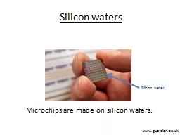
PPT-Silicon Wafer Japan TC Chapter Liaison Report
Author : alexa-scheidler | Published Date : 2018-10-31
For NA Silicon Wafer TC Chapter Meeting In conjunction with NA Spring Standards Meetings 2 Leadership Committee Cochairs Naoyuki J Kawai Independent Tet s uya Nakai
Presentation Embed Code
Download Presentation
Download Presentation The PPT/PDF document "Silicon Wafer Japan TC Chapter Liaison R..." is the property of its rightful owner. Permission is granted to download and print the materials on this website for personal, non-commercial use only, and to display it on your personal computer provided you do not modify the materials and that you retain all copyright notices contained in the materials. By downloading content from our website, you accept the terms of this agreement.
Silicon Wafer Japan TC Chapter Liaison Report: Transcript
For NA Silicon Wafer TC Chapter Meeting In conjunction with NA Spring Standards Meetings 2 Leadership Committee Cochairs Naoyuki J Kawai Independent Tet s uya Nakai SUMCO Leadership Changes. By:. Martin . Friedl. Jeremy . Miller. Michael . Sawires. . Research in Sputtered Amorphous Silicon . Thin Film Solar Cells. The Current State of Solar Power. “Total installed [photovoltaic] capacity in the world now amounts to around 40 GW, producing some 50 terawatt-hours (. n. : . The . Genesis Allocation Committee received a request for a . ~ . 1 cm. 2. piece of the diamond-like-carbon (DLC) concentrator target for the analysis of solar wind nitrogen isotopes. An estimated 75% of the DLC target was recovered in at least 18 fragments following the off nominal return of the Genesis spacecraft in 2004. The largest fragment, 60000, was designated for this allocation and is the first space exposed flight sample to be subdivided using the ARES laser scribing system. . of. Information & Control Global Technical Committee Liaison Report. April 1, 2015. R.0.2a. To: North America TC Chapter of Information & Control Global Technical Committee. Leadership and Structure Change. Werner Bergholz, Jacobs University Bremen. Friedrich Passek, . Siltronic. AG. Peter Wagner. Updated . October 23, 2014. Task . Forces. . with. European . Participation. Int. . Advanced. Wafer . Geometry. . 1. Semiconductor Manufacturing Technology: . Semiconductor Manufacturing Processes. Conrad T. Sorenson. Praxair, Inc.. . 1999 Arizona Board of Regents for The University of Arizona. NSF/SRC Engineering Research Center for Environmentally Benign Semiconductor Manufacturing. After procuring raw sand and separating the silicon, the excess material is disposed of and the silicon is purified in multiple steps to finally reach semiconductor manufacturing quality which is called electronic grade silicon. The resulting purity is so great that electronic grade silicon may only have one alien atom for every one billion silicon atoms. After the purification process, the silicon enters the melting phase. In this picture you can see how one big crystal is grown from the purified silicon melt. The resulting mono-crystal is called an ingot.. SGS, Crystal Defects & Wafer. Preparation . . Guided By. MD. Mohiuddin Munna. . #Group Members#. Chinmoy Das (2010338012). Nazmul Hossain (2010338016). Dr. . Esam. . Yosry. Lec. . #6. Lithography. Introduction. Lithography. Photolithography. Photoresist Process. Types of Photoresist. Photomask. Clean Rooms. . Introduction. (. Chip Fabrication Cycle). of thin silicon cooling plates. 4” silicon wafer 380 µm thick. Partial etching of manifolds. 380 µm. Etching of channels and manifolds. Channels. 200 x 70 µm. Fins. 200 µm. Manifolds. 280 µm deep. cooling - Update. 07 Sep 2010. 1. G. Nüßle. Outline. Test . of. 1st . full-scale. prototype. Hydraulic. . behaviour. Thermal . behaviour. Layout . optimization. . for. . the. prototype. Structural. isotropic. and . anisotropic etching. Explain the differences between . wet. . and . dry etching. techniques. Identify several common wet etchants and explain what they are commonly used for. Explain the difference between . it—Part 1. Explain . how single crystalline Si wafers are made . Describe . the crystalline structure of Si . Find . the . Miller indices. of a planes and directions in crystals and give the most important direction/planes in silicon . Genesis Allocation Committee received a request for a . ~ . 1 cm. 2. piece of the diamond-like-carbon (DLC) concentrator target for the analysis of solar wind nitrogen isotopes. An estimated 75% of the DLC target was recovered in at least 18 fragments following the off nominal return of the Genesis spacecraft in 2004. The largest fragment, 60000, was designated for this allocation and is the first space exposed flight sample to be subdivided using the ARES laser scribing system. Module #4 – CMOS Fabrication. Agenda. CMOS Fabrication. - Yield. - Process Steps for MOS transistors. - Inverter Example. - Design Rules. - Passive Components. - Packaging. Announcements.
Download Document
Here is the link to download the presentation.
"Silicon Wafer Japan TC Chapter Liaison Report"The content belongs to its owner. You may download and print it for personal use, without modification, and keep all copyright notices. By downloading, you agree to these terms.
Related Documents