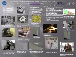
PPT-Silicon Wafer Committee Europe
Author : mitsue-stanley | Published Date : 2015-12-10
Werner Bergholz Jacobs University Bremen Friedrich Passek Siltronic AG Peter Wagner Updated October 23 2014 Task Forces with European Participation Int Advanced
Presentation Embed Code
Download Presentation
Download Presentation The PPT/PDF document "Silicon Wafer Committee Europe" is the property of its rightful owner. Permission is granted to download and print the materials on this website for personal, non-commercial use only, and to display it on your personal computer provided you do not modify the materials and that you retain all copyright notices contained in the materials. By downloading content from our website, you accept the terms of this agreement.
Silicon Wafer Committee Europe: Transcript
Werner Bergholz Jacobs University Bremen Friedrich Passek Siltronic AG Peter Wagner Updated October 23 2014 Task Forces with European Participation Int Advanced Wafer Geometry. By:. Martin . Friedl. Jeremy . Miller. Michael . Sawires. . Research in Sputtered Amorphous Silicon . Thin Film Solar Cells. The Current State of Solar Power. “Total installed [photovoltaic] capacity in the world now amounts to around 40 GW, producing some 50 terawatt-hours (. n. : . The . Genesis Allocation Committee received a request for a . ~ . 1 cm. 2. piece of the diamond-like-carbon (DLC) concentrator target for the analysis of solar wind nitrogen isotopes. An estimated 75% of the DLC target was recovered in at least 18 fragments following the off nominal return of the Genesis spacecraft in 2004. The largest fragment, 60000, was designated for this allocation and is the first space exposed flight sample to be subdivided using the ARES laser scribing system. Peter W Phillips. 12/03/2014. ABC130 Wafer Probe. Three projects competing for time on RAL Cascade S3000 probe station. Try older Micromanipulator station instead. Originally bought for . “The . R. SGS, Crystal Defects & Wafer. Preparation . . Guided By. MD. Mohiuddin Munna. . #Group Members#. Chinmoy Das (2010338012). Nazmul Hossain (2010338016). Dr. . Esam. . Yosry. Lec. . #6. Lithography. Introduction. Lithography. Photolithography. Photoresist Process. Types of Photoresist. Photomask. Clean Rooms. . Introduction. (. Chip Fabrication Cycle). of thin silicon cooling plates. 4” silicon wafer 380 µm thick. Partial etching of manifolds. 380 µm. Etching of channels and manifolds. Channels. 200 x 70 µm. Fins. 200 µm. Manifolds. 280 µm deep. cooling - Update. 07 Sep 2010. 1. G. Nüßle. Outline. Test . of. 1st . full-scale. prototype. Hydraulic. . behaviour. Thermal . behaviour. Layout . optimization. . for. . the. prototype. Structural. Topic 4.2.9 – 4.2.10. 2. characteristics. some elements from group 4 are . giant. molecules. carbon and silicon . insoluble in almost all solvents. h. igh melting and boiling points. Carbon allotropes . AGH University of Science and Technology. . Faculty of Physics and Applied Computer Science, . Kraków. , Poland. Jagiellonian. . Symposium. 2015 7-12/06/2015. Silicon wafer. www.guardian.co.uk. http://. mrsec.wisc.edu. en.wikipedia.org. Wafers are cut from . boules. , . which are large . logs . of uniform . silicon.. Looking at this picture, . where. do you think silicon . Swaroop K. Behera. 1. , . Shvetashwa. Suri. 1. Pradeep Rohatgi. 1. , Nathan Salowitz. 2. 1. Department of Material Science and Engineering, UW-Milwaukee . 2. Department of Mechanical Engineering , UW-Milwaukee. It is very significant to be the safe and healthy lifestyle. There is the huge demand for Oasis medical services in the present time because they are well known for their admirable dedicated health care services. For NA Silicon Wafer TC Chapter Meeting. In conjunction with NA Spring Standards Meetings . 2. Leadership. Committee Co-chairs. Naoyuki. J. Kawai/ Independent. Tet. s. uya Nakai/ SUMCO. Leadership Changes. Genesis Allocation Committee received a request for a . ~ . 1 cm. 2. piece of the diamond-like-carbon (DLC) concentrator target for the analysis of solar wind nitrogen isotopes. An estimated 75% of the DLC target was recovered in at least 18 fragments following the off nominal return of the Genesis spacecraft in 2004. The largest fragment, 60000, was designated for this allocation and is the first space exposed flight sample to be subdivided using the ARES laser scribing system.
Download Document
Here is the link to download the presentation.
"Silicon Wafer Committee Europe"The content belongs to its owner. You may download and print it for personal use, without modification, and keep all copyright notices. By downloading, you agree to these terms.
Related Documents