/
IEEE TRANSACTIONS ON CIRCUITS AND SYSTEMSII ANALOG AND DIGITAL SIGNAL PROCESSING VOL IEEE TRANSACTIONS ON CIRCUITS AND SYSTEMSII ANALOG AND DIGITAL SIGNAL PROCESSING VOL

IEEE TRANSACTIONS ON CIRCUITS AND SYSTEMSII ANALOG AND DIGITAL SIGNAL PROCESSING VOL - PDF document

briana-ranney
briana-ranney . @briana-ranney
Follow
515 views
Uploaded On 2014-12-22

IEEE TRANSACTIONS ON CIRCUITS AND SYSTEMSII ANALOG AND DIGITAL SIGNAL PROCESSING VOL - PPT Presentation

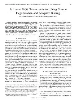
48 NO 10 OCTOBER 2001 937 A Linear MOS Transconductor Using Source Degeneration and Adaptive Biasing KoChi Kuo Member IEEE and Adrian Leuciuc Member IEEE Abstract This paper presents a new configuration for linear MOS voltagetocurrent conversion t ID: 27807

OCTOBER

Share:

Link:

Embed:

Download Presentation from below link

Download Pdf The PPT/PDF document "IEEE TRANSACTIONS ON CIRCUITS AND SYSTEM..." is the property of its rightful owner. Permission is granted to download and print the materials on this web site for personal, non-commercial use only, and to display it on your personal computer provided you do not modify the materials and that you retain all copyright notices contained in the materials. By downloading content from our website, you accept the terms of this agreement.


Presentation Transcript

IEEETRANSACTIONSONCIRCUITSANDSYSTEMS—II:ANALOGANDDIGITALSIGNALPROCESSING,VOL.48,NO.10,OCTOBER2001937ALinearMOSTransconductorUsingSourceDegenerationandAdaptiveBiasingKo-ChiKuo,Member,IEEE,andAdrianLeuciuc,Member,IEEEThispaperpresentsanewconfigurationforlinearMOSvoltage-to-currentconversion(transconductance).Theproposedcircuitcombinestwopreviouslyreportedlinearizationmethods[1],[2].Thetopologyachieves60-dBlinearityforafullybalancedinputdynamicrangeupto1 -C.Active-configurationsuseop-amps,andresistorsandcapacitorsaspassivefrequency-determiningcomponents.Theypresentverygoodlinearity,butusuallyrequirelargedieareaforresistorsand/orcapacitors,thetuningcanbeachievedonlyinadiscretemannerbyusingarraysofpassivecomponents,andthelargevalueresistorscanintroducesubstantiallythermalnoise.Anotherclassofcontinuous-timefiltersisderivedfromclassicalactive-filtersandusesMOSfield-effecttransistors(MOSFETs),capacitors,andop-amps.TheyarethusreferredtoasMOSFET-Cactivefilters[3],[4].TheseimplementationshavepoorlinearityduetothenonlinearcharacteristicoftheMOStransistors.Althoughthelinearitycanbeimprovedby 40dBfor0.7 atasingle5-Vsupply.Theuseoftransconductorsandcapacitorstoimplementintegratorsisanothertechniquetorealizecontinuous-timeManuscriptreceivedOctober13,2000;revisedOctober12,2001.ThisworkwassupportedbytheCenterforDesignofAnalog-DigitalIntegratedCircuits(CDADIC).ThispaperwasrecommendedbyAssociateEditorG.Cauwen-berghs. -Cconfigurations[7],[8]havebetterfrequencyresponsecomparedtoactive-RCandMOSFET-Crealizationsduetotheabsenceoflocalfeedbackaroundtheactiveele-ments.Theyhavealsoelectronictuningcapability,butarecharacterizedbyaratherpoorlinearity.Therefore,additionalcircuitryisneededtolinearizethetransfercharacteristicofatransconductor.SinceG -Cconfigurationshavebetterfrequencyresponseandusuallywidertuningrange,theyarenowadaysamongthemostpopularapproachesforimplementingintegratedcontinuous-timefilters.SeveralcircuittechniqueshavebeenproposedinliteraturetoimprovethelinearityofbipolarandMOStransconductors.InthiscommunicationwewillreferonlytoMOStransconductors,agoodsurveyonmostofthelinearizationtechniquesbeinggivenin[9].Thelinearizationmethodsinclude:cross-couplingofmultipledifferentialpairs[2],[10],[11],adaptivebiasing[2],[12],sourcedegeneration(usingresistorsorMOStransistors)[1],[13],[14],shiftlevelbiasing[15],seriesconnectionofmultipledifferentialpairs[16],andpseudodifferentialstages(usingtransistorsinthetrioderegionorinsaturation)[17],[18].ThispaperpresentsanimprovedlinearMOStransconductorthatusesboththeadap- process,usingasingle3.3-Vsupplyvoltage.Experimentalresultsareincludedforcomparisontothesimulationresults.SomefinalconclusionsarepresentedinSectionIV.II.COPOLOGIESFORRANSCONDUCTORSInthissection,wewillfirstreviewthreelinearizationtech-niquespreviouslyreportedinliterature.ThefirstoneistheMOSdifferentialpairwithresistivesourcedegeneration.Thesecond – characteristicsfortheMOStransistorsinthesaturationre-1057–7130/01$10.00©2001IEEE 938IEEETRANSACTIONSONCIRCUITSANDSYSTEMS—II:ANALOGANDDIGITALSIGNALPROCESSING,VOL.48,NO.10,OCTOBER2001 Fig.1.(a)SimpledifferentialMOStransconductor.(b)MOStransconductorwithresistivesourcedegeneration.gionandthechannellengthmodulationeffectwillbeneglectedforsimplicity.Therefore,thedraincurrentisgivenby (1)where isthetransconductanceparameterand isthethresholdvoltageoftheMOStransistor.Using(1)thesimpledifferentialMOStransconductorshowninFig.1(a)hasatransfercharacteristicgivenby Betterlinearitycanbeachievedforlargeeffectivegate-to-sourcevoltages, .Forlow-voltageapplica-tionsthisconstitutesamajordrawback.Oneofthesimplesttopologiestolinearizethetransferchar-acteristicoftheMOStransconductoristheonewithsourcede-generationusingresistorsanddepictedinFig.1(b).Thedisad-vantageofthisconfigurationisthelargeresistorvalueneededtoachieveawidelinearinputrange.Sinceinthiscase ,theobtainedtransconductanceisrestrictedtosmallvalues.Moreover,thistechniqueeliminatestheelectronictuningcapa-bilityofthetransconductancebecauseitsvalueissetbythede-generationresistor.B.MOSTransconductorsWithSourceDegenerationUsingMOSTransistorsByreplacingthedegenerationresistorswithtwoMOStran-sistorsoperatinginthetrioderegion,thecircuitinFig.2isobtained.Consideringperfectlymatchedtransistors – , – ,andneglectingthebodyandchannellengthmodula-tioneffects,thetransfercharacteristicofthistransconductorisgivenby (3)where Usually,thenonlineartermunderthesquarerootcanbemademuchsmallerthanunityandimprovedlinearityandlargerinput Fig.2.MOStransconductorwithsourcedegenerationusingMOStransistors.dynamicrangecanbeobtained.However,increasedlinearitymeanssmallerequivalenttransconductanceandreducedtuningcapability.Thecircuithasbandwidthandnoiseperformancescomparabletothesimpledifferentialpair.Whentheinputvoltageincreasesbeyondacertainvalue oneofthetwodegenerationtransistorsentersinthesaturationregion( for ,respectively for ).Theoutputdifferentialcurrentinthiscaseisgivenby InFig.3(a)therelativeerrorofthetransconductance derivedfromeqs.(3)–(6)isplottedfordifferentvaluesofparameter .Itcanbeeasilyseenanditwasalsoshownin[1]thatonecanincreasetheinputlineardynamicrangebyappro-priatelysettingthevalueofparameter (somewherebetween2.5and2.75).However,thenonlinearityerrorisupto1%for %.InsomefilteringapplicationsitisrequiredtohavebetterlinearityinordertoachieveaTHDof 60dBorC.AdaptivelyBiasedMOSTransconductorsAnothertopologytoachievehighfrequencylinearMOStransconductorswasreportedin[2].Theideaistouseatailcurrentcontaininganinputdependentquadraticcomponenttocancelthenonlineartermin(2).Thus,if thetransfercharacteristicbecomeslinear Therequiredbiasingcurrentcanbeeasilyobtainedusingan-othertwoMOStransistors – havingidenticaltranscon-ductancecoefficientsastheonesinthedifferentialpair – andtwounit-gaincurrentmirrors – and – asitisshowninFig.4.Additionalcircuitryisneededforgeneratingthetuningvoltage .Thenoisegeneratedbythesquaringcir-cuitrydoesnotappearattheoutputofthetransconductorsinceitislikeacommonmodevoltageatthesourcesofthedifferential KUOANDLEUCIUC:LINEARMOSTRANSCONDUCTOR Fig.3.RelativetransconductanceerrorfortheMOStransconductors.(a)UsingsourcedegenerationwithMOStransistors.(b)UsingsourcedegenerationwithMOStransistorsandadaptivebiasing.Parameterisvariedwithastepof0.25. Fig.4.AdaptivelybiasedMOStransconductor.pair.Itwasshownin[9]thatduetotheeffectofmobilityreduc-tion,thesizeofthetransistorsinthesquaringcircuitryshouldbecomputedasafunctionofthevoltage inordertoob-tainthebestlinearity.Therefore,tuningthecircuitbymeans willworsenthelinearity.Theclassofinputsignals Fig.5.ProposedlinearMOStransconductor.whichcanbeprocessedislimitedsincetherequirementoffullybalancedsignalsisneededforthesquaringcircuittofunctionproperly[9].D.ALinearMOSTransconductorUsingSourceDegenerationandAdaptiveBiasingWeproposeanotherMOStransconductorthatcombinesthetwolinearizationapproachespresentedabove.Startingfromcir-cuitinFig.2andusingadaptivebiasingcurrentsources,thecir-cuitdepictedinFig.5isobtained.Totransformthenonlineartransfercharacteristic(3)intoalinearone,thetailcurrent shouldhavetheexpression Thetransfercharacteristicbecomeslinearandisgivenby Theadaptivebiascurrentis Comparing(9)and(11),thetransconductancecoefficientofthesquaringcircuitshouldbe (12)Since issmallerthan ,thedccomponentofthecurrentgeneratedbythesquaringcircuitryissmallcomparedtothenec-essaryvaluerequiredtobiasthedifferentialpair.Therefore,anadditionalcurrentsource isneededtotunethetranscon-ductor.Whentheinputvoltageincreasesabovethevalue (13) 940IEEETRANSACTIONSONCIRCUITSANDSYSTEMS—II:ANALOGANDDIGITALSIGNALPROCESSING,VOL.48,NO.10,OCTOBER2001oneofthetransistors , entersinthesaturationregionandtheoutputdifferentialcurrentisgivenby Fig.3(b)showsthecomputedrelativetransconductanceerrorforthecircuitinFig.5,assumingquadraticMOS – istics(1).Imposingacertainmaximumnonlinearityerror,thevalueofparameter canbecomputed.Inpractice,deviationsfromthequadraticMOS – characteristicduetomobilityre-ductionandthebodyeffectcauseincompletecancellationin(3).Therefore,thetransconductancecharacteristicpresentsacertaincurvatureevenforthecasewhenbothtransistors – areinthetrioderegion.SPICEsimulationsusingBSIM3v3MOSFETmodelshaveshownthatthebestlinearitycanbeachievedbysettingthevalueoftheparameter between1.5and1.75.III.SIMULATIONANDXPERIMENTALESULTSA.ComparisonofDifferentLinearizationTechniquesInordertocomparetheperformanceofdifferentlineariza-tiontechniques,numerouscomputersimulationshavebeenrun.Toobtainafairandaccuratecomparison,thecircuitspresentedinSectionIIhavebeenoptimizedtoachievethebestlinearitypossibleforagiventransconductancevalue.SPICEsimulatedtransconductanceasafunctionoftheinputdifferentialvoltageisplottedinFig.6.FromthedetailshowninFig.6(b)itcanbeeasilyseenthatthelinearityachievedbythenewlyproposedconfigurationisbetterthanalltheotherones.Thefigurealsoin-cludedtheresultsobtainedinthecaseofatransconductorwithresistivesourcedegenerationandadaptivebiasing,forcompar-isonpurposes.TheTHDoftheoutputdifferentialcurrentversustheampli-tudeoftheinputvoltageforthethreetransistor-onlylinearizedtransconductorsisdepictedinFig.7.ThetopologyinFig.4achievesTHDlessthan 57dBfor1.6 inputvoltage,10dBbetterthantheonewithoutadaptivebiasingand27dBbetterthantheoneusingonlyadaptivebiasing,forthesameinputrange.Forthesamedesignedtransconductancevalue,thenovelproposedconfigurationisthesecondbestasfarasthepowerconsumptionanddiearea.ItissurpassedonlybythecircuitinFig.4forwhichthelinearityisstronglydependentonthetuningvoltage.Fig.8illustratesthelinearityperformanceofthethreetran-sistor-onlytransconductorswhentunedforseveraltransconduc-tancevalues.ThetransconductorinFig.4istunedbychanging ,theoneinFig.2bychangingthetailcurrents ,andthenewlyproposedonebychanging .Ourapproachisagainthebestone.Sincethesquaringcircuitryusedinadaptivebiasingisprop-erlyfunctioningonlyforfullybalancedinputs,thebehavioroftheMOStransconductorshasbeenstudiedinthecaseofun-balancedinputaswell.Becausethequadraticcomponentofthe Fig.6.Simulatedtransconductanceforfivelinearizationtechniques.(a)Fullplot.(b)Detail.( )resistivesourcedegeneration;()resistivesourcedegenerationwithadaptivebiasing;()sourcedegenerationusingMOStransistors;( )adaptivebiasing;()sourcedegenerationusingMOStransistorsandadaptivebiasing. Fig.7.SimulatedTHDat1kHzforthethreeresistor-freelinearizationtechniques.( )sourcedegenerationusingMOStransistors;( )adaptivebiasing;()sourcedegenerationusingMOStransistorsandadaptivebiasing.adaptivebiasingcurrentfortheproposedcircuitissmallerthantheoneneededfortheconfigurationinFig.4[see(7)and(9)],thelinearityofthenewlyintroducedtransconductordegrades KUOANDLEUCIUC:LINEARMOSTRANSCONDUCTOR Fig.8.SimulatedtransconductanceofthreelinearizedMOStransconductorsundertuning.(a)SourcedegenerationusingMOStransistors.(b)Adaptivebiasing.(c)SourcedegenerationusingMOStransistorsandadaptivebiasing.lessforunbalancedinputs.TheobtainedsimulationresultsaredepictedinFig.9andtheyconfirmtheexpectedbehavior.B.ExperimentalResultsThelinearMOStransconductorhasbeenfabricatedusingthe mprocessfromTSMC.ThediagramoftheentirecircuitisshowninFig.10.Theactiveload – iscontrolledbythecommonmodefeedbackcircuitryforadjustingtheoutput Fig.9.Simulatedtransconductanceforthethreeresistor-freelinearizationtechniquesinthecaseofunbalancedinput.(a)SourcedegenerationusingMOStransistors.(b)Adaptivebiasing.(c)SourcedegenerationusingMOStransistorsandadaptivebiasing.( )fullybalanced;()20%unbalanced; )40%unbalanced;()60%unbalanced;()80%unbalanced;()100%commonmodevoltagetothedesiredvalue .Transistors – supplythevoltage and generates Tuningcanbeachievedbymeansofthetriodetransistor Thestart-upcircuitryneededforthebiasingparthasbeenomittedinFig.10.Thefabricatedprototypehasbeendesignedforuseinacon-tinuous-timelow-passdelta-sigmamodulator.Verylargearea 942IEEETRANSACTIONSONCIRCUITSANDSYSTEMS—II:ANALOGANDDIGITALSIGNALPROCESSING,VOL.48,NO.10,OCTOBER2001 Fig.10.Fullcircuitdiagramofthefabricatedtransconductor. Fig.11.Simulated(dottedlines)andmeasured(continuouslines)dcresponse.transfercharacteristic.(b)Transconductance.transistorsareusedintheoutputstagetominimize withanactiveareaof0.47mm fortheentiretransconductor.Asinglesupplyvoltageof3.3Vhasbeenusedandtheentiretransconductordissipates1mWfor and5-MHzbandwidth.Therelativelowvalueofthetransconductanceislimitedbytheapplication,andreducestheinputlinearrangecomparedtotheoptimalvaluesobtainedforthesimulationsintheprevioussection.ThesimulatedandmeasureddccharacteristicsareshowninFig.11.Thetransconductanceplothasbeenobtainedbydiffer-entiatingthemeasuredoutput – characteristic.Therippleiscausedbythesmallnumberofpointsandfiniteprecisionofthemeasurement.ThemeasuredTHDisapproximately6to10dBlargerthanthesimulatedone.Thisiscausedbythenonperfectmatchingofthetransistorsand,possibly,bytheadditionaldis-tortionsintroducedbythedifferentialtosingle-endedconver-sioncircuitryusedinthemeasurementsetup.IV.CAnimprovedlinearMOStransconductor,combiningtwolinearizationmethodshasbeenpresented.ThetopologycanachievebetterlinearitycomparedtootherapproachesanditcanbeusedinimplementingfullydifferentialG -Ccon-tinuous-timefilterswithseverelinearityrequirements.Theproposedcircuithasgoodtuningcapabilityanditfunctionsforbothfully-balancedandunbalancedinputsignals,withsomelinearitydepreciationinthelattercase.Inapracticalimplementation,thefinallinearityperformanceissetbythematchingprecisionoftheMOSFETs.Theproposedcircuithasbeenfabricatedandexperimentalresultsagreewithsimulatedlinearityperformance.[1]F.KrummenacherandN.Joehl,“A4-MHzCMOScontinuous-timefilterwithon-chipautomatictuning,”IEEEJ.Solid-StateCircuits,vol.23,pp.750–758,June1988.[2]A.NedungadiandT.R.Viswanathan,“DesignoflinearCMOStransconductanceelements,”IEEETrans.CircuitsSyst.,vol.CAS-31,pp.891–894,Oct.1984.[3]Y.TsividisandM.Banu,“Continuous-timeMOSFET-CfiltersinIEEEJ.Solid-StateCircuits,vol.SC-21,pp.15–30,Feb.1986.[4]M.BanuandY.Tsividis,“FullyintegratedactiveRCfiltersinMOStechnology,”IEEEJ.Solid-StateCircuits,vol.SC-18,pp.644–651,Dec.[5]Z.Czarnul,“ModificationofBanu–Tsividiscontinuous-timeinte-grator,”IEEETrans.CircuitsSyst.,vol.CAS-33,pp.714–716,July[6]G.Groenewold,“Thedesignofhighdynamicrangecontinuous-timeintegratablebandpassfilters,”IEEETrans.CircuitsSyst.,vol.38,pp.838–852,Aug.1991.[7]H.KhorramabadiandP.R.Gray,“High-frequencyCMOScon-tinuous-timefilters,”IEEEJ.Solid-StateCircuits,vol.SC-19,pp.939–948,Dec.1984. KUOANDLEUCIUC:LINEARMOSTRANSCONDUCTOR[8]F.Krummenacher,“Designconsiderationinhighfrequency,CMOSTransconductanceAmplifierCapacitor(TAC)filters,”inProc.IEEEInternationalSymp.CircuitsSyst.ISCAS’89,1989,pp.100–105.[9]S.T.DupuieandM.Ismail,“HighfrequencyCMOStransconductors,”AnalogueICDesign:TheCurrent-ModeApproach,C.Toumazou,F.J.Lidgey,andD.G.Haigh,Eds.London,U.K.:PeterPeregrinus,[10]H.Khorramabadi,“HighfrequencyCMOScontinuoustimefilter,”Ph.D.dissertation,Univ.California,Berkeley,1985.[11]E.SeevinckandR.F.Wassenaar,“AversatileCMOSlineartranscon-ductor/square-lawfunctioncircuit,”IEEEJ.Solid-StateCircuits,vol.SC-22,pp.366–377,June1987.[12]M.G.Degrauwe,J.Rijmenants,E.A.Vittoz,andH.J.DeMan,“Adap-tivebiasingCMOSamplifiers,”IEEEJ.Solid-StateCircuits,vol.SC-17,pp.522–528,June1982.[13]D.R.Welland,“Transconductanceamplifiersandexponentialvariablegainusingthesame,”U.S.Patent5451901,Sept.19,1995.[14]I.MehrandD.R.Welland,“ACMOScontinuous-time filterforPRMLreadchannelapplicationsat150Mb/sandbeyond,”IEEEJ.Solid-StateCircuits,vol.32,pp.499–513,Apr.1997.[15]Z.WangandW.Guggenbuhl,“Avoltage-controlledlinearMOStransconductorusingbiasoffsettechnique,”IEEEJ.Solid-StateCircuits,vol.25,pp.315–317,Feb.1990.[16]J.Silva-Martinez,M.S.J.Steyaert,andW.Sansen,“A10.7-MHz68-dBSNRCMOScontinuous-timefilterwithon-chipautomaticIEEEJ.Solid-StateCircuits,vol.27,pp.1843–1852,Dec.[17]R.Alini,A.Baschirotto,andR.Castello,“TunableBiCMOScontin-uous-timefilterforhigh-frequencyapplications,”IEEEJ.Solid-StateCircuits,vol.27,pp.1905–1915,Dec.1992.[18]S.L.Wong,“Noveldrain-basedtransconductancebuildingblocksforcontinuous-timefilterapplications,”Electron.Lett.,vol.25,no.2,pp.100–101,Jan.1989. Ko-ChiKuo(S’93–M’01)receivedtheDiplomainelectronicengineeringfromMingHsinEngineeringCollege,Hsin-Chu,Taiwan,R.O.C.,in1987,theM.S.degreefromTulaneUniversity,NewOrleans,LA,andthePh.D.degreefromtheStateUniversityofNewYorkatStonyBrook,bothinelectricalengineering,in1994and2001,respectivelyFrom1994and2001,hewaswiththeDepartmentofElectricalandComputerEngineering,theStateUniversityofNewYorkatStonyBrook.Currently,heisaStaffEngineerwiththeCommunicationRe-searchandDevelopmentCenter(CRDC),BostonDesignCenter,IBM,Lowell,MA.Hiscurrentresearchinterestsincludehighperformancedigitalcircuitdesign,lineartransconductors,mixedsignalcircuitdesign,andPLL/FrequencySynthesizersinwirelesscommunications.Dr.KuoisamemberofEtaKappaNu. AdrianLeuciuc(M’99)receivedtheDipl.Eng.(M.Sc.)andPh.D.DegreesinelectronicengineeringfromtheTechnicalUniversityofIasi,Romania,in1990and1996,respectively.From1991and1997,hewaswiththeDepartmentofElectronicsandTelecommunications,TechnicalUniversityofIasi,Romania.In1998,hewasaVisitingProfessorwiththeDepartmentofElectricalandComputerEngineering,theStateUniversityofNewYorkatStonyBrook,thenbecameanAssistantProfessorwiththesamedepartment.Hisresearchinterestsincludecontinuous-timefilters,dataconverters,nonlinearandchaoticcircuitsandtheirapplicationsincommunications.Dr.LeuciucisamemberofEtaKappaNu.