PDF-15 years of graphene electronicsWork on twodimensional materials cont
Author : brooke | Published Date : 2021-07-07
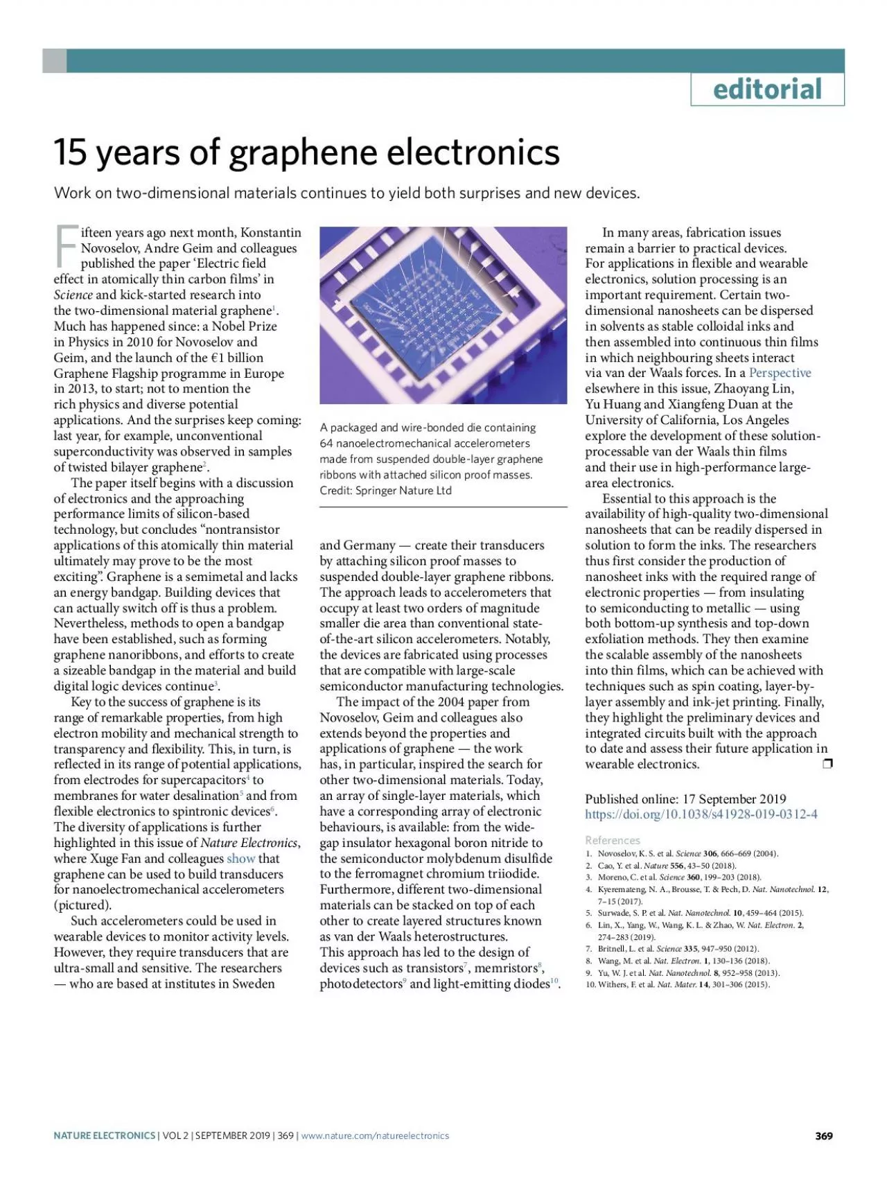
369 A packaged and wirebonded die containing 64 nanoelectromechanical accelerometers made from suspended doublelayer graphene ribbons with attached silicon proof
Presentation Embed Code
Download Presentation
Download Presentation The PPT/PDF document "15 years of graphene electronicsWork on ..." is the property of its rightful owner. Permission is granted to download and print the materials on this website for personal, non-commercial use only, and to display it on your personal computer provided you do not modify the materials and that you retain all copyright notices contained in the materials. By downloading content from our website, you accept the terms of this agreement.
15 years of graphene electronicsWork on twodimensional materials cont: Transcript
Download Rules Of Document
"15 years of graphene electronicsWork on twodimensional materials cont"The content belongs to its owner. You may download and print it for personal use, without modification, and keep all copyright notices. By downloading, you agree to these terms.
Related Documents