PPT-Graphene & Nanowires: Applications
Author : kittie-lecroy | Published Date : 2018-11-01
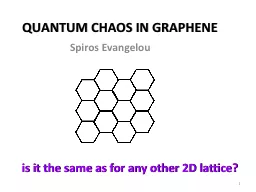
Kevin Babb amp Petar Petrov Physics 141A Presentation March 5 2013 What is a Nanowire Onedimensional structure Diameter 1100 nanometers 10 9 m Length microns 10
Presentation Embed Code
Download Presentation
Download Presentation The PPT/PDF document "Graphene & Nanowires: Applications" is the property of its rightful owner. Permission is granted to download and print the materials on this website for personal, non-commercial use only, and to display it on your personal computer provided you do not modify the materials and that you retain all copyright notices contained in the materials. By downloading content from our website, you accept the terms of this agreement.
Graphene & Nanowires: Applications: Transcript
Download Rules Of Document
"Graphene & Nanowires: Applications"The content belongs to its owner. You may download and print it for personal use, without modification, and keep all copyright notices. By downloading, you agree to these terms.
Related Documents