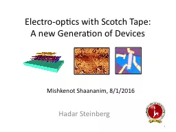
PPT-= Areas with graphene
Author : giovanna-bartolotta | Published Date : 2016-09-03
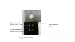
Scratch Mark For Gating Device Nearest to Gating scratch TOP Device Furthest from Gating scratch Bottom Dneff 7272015 Co3970 application to UCI Burke lab graphene
Presentation Embed Code
Download Presentation
Download Presentation The PPT/PDF document "= Areas with graphene" is the property of its rightful owner. Permission is granted to download and print the materials on this website for personal, non-commercial use only, and to display it on your personal computer provided you do not modify the materials and that you retain all copyright notices contained in the materials. By downloading content from our website, you accept the terms of this agreement.
= Areas with graphene: Transcript
Download Rules Of Document
"= Areas with graphene"The content belongs to its owner. You may download and print it for personal use, without modification, and keep all copyright notices. By downloading, you agree to these terms.
Related Documents