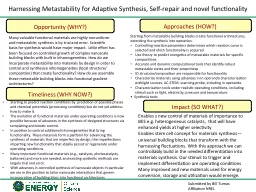
Emily Threatt Cameron Jeske Ali Mohsin Dr Gong Gu Wan Deng Christian Academy of Knoxville Hardin Valley Academy The University of Tennessee Knoxville SPONSORS This work was supported in part by the Engineering Research Center Pr ID: 277689
Download Presentation The PPT/PDF document "Exfoliation and Synthesis of 2D Material..." is the property of its rightful owner. Permission is granted to download and print the materials on this web site for personal, non-commercial use only, and to display it on your personal computer provided you do not modify the materials and that you retain all copyright notices contained in the materials. By downloading content from our website, you accept the terms of this agreement.
Slide1
Exfoliation and Synthesis of 2D Materials
Emily Threatt, Cameron Jeske, Ali Mohsin, Dr. Gong Gu, Wan DengChristian Academy of Knoxville, Hardin Valley Academy, The University of Tennessee- Knoxville
SPONSORS: This work was supported in part by the Engineering Research Center, Program of the National Science Foundation, and the Department of Energy under NSF Award Number EEC-1041877 and the CURENT Industry Partnership Program.
Objectives
The objective of our project is to research the properties of 2D materials, and their application to electronic devices.
Background
Graphene- was the primary material that we researched.single atom thickarranged in a honeycomb latticestrongest material in existenceflexibletransparentconductiveExfoliationExfoliation is the act of separating layered materials such as graphene or molybdenum disulfide into thin layers.Achieved by placing material on Scotch tape, and repeatedly folding the tape back onto itself, thus separating it into smaller layers. Material used to exfoliate: molybdenum disulfide (MoS2) MoS2 a hexagonal shape similar to graphene.Exfoliation is used to study the material, and to make proof of concept devices. SEMSEM: Scanning Electron Microscope. A SEM works by focusing a beam of electrons onto an object. The primary electrons get scattered, resulting in secondary electrons that are collected by the detector for imaging. The dark area is the graphene. The hexagonal structure is vaguely visible. Boron nitride appears as a triangle. The star-like formations are the boding of multiple boron nitride atoms. Electronic DevicesThe main electronic devices that graphene is applied are transistors.Graphene TransistorThese devices are tested by setting probes on the two pieces of metal, and running an electrical current. If the current remains unbroken, the graphene has made a good connection. ApplicationThe transistor isn’t the only device that graphene is used for. For example, Samsung has released a model for a mobile phone, utilizing the flexible properties of graphene.
100µm
100µm
100 micrometers