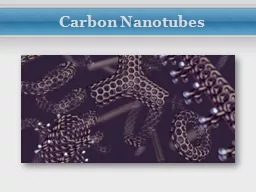
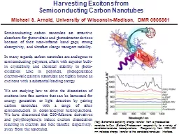
Discovered in 1991 by Sumiyo Iijima a Japanese scientist working at the NEC Corporation Is a tubular form of carbon with a diameter as small as 04 nm and length from a few nanometers up to a millimeter ID: 758522
Download Presentation The PPT/PDF document "Carbon Nanotubes CARBON NANOTUBES" is the property of its rightful owner. Permission is granted to download and print the materials on this web site for personal, non-commercial use only, and to display it on your personal computer provided you do not modify the materials and that you retain all copyright notices contained in the materials. By downloading content from our website, you accept the terms of this agreement.
Slide1
Carbon NanotubesSlide2
CARBON NANOTUBES
Discovered in 1991 by
Sumiyo
Iijima
, a Japanese scientist working at the NEC Corporation.
Is a tubular form of carbon with a diameter as small as 0.4 nm and length from a few nanometers up to a millimeter.
Length-to-diameter ratio of a carbon nanotube can be as large as 28,000,000:1, which is unequalled by any other material.
Carbon exists in several forms; graphite and diamond are the most familiar.
A CNT is characterized by its
Chiral
Vector:
C
h
= n
â
1
+ m
â
2
,
Slide3
Formation of CNT
Process which is used to form these Nanotubes, is called
Chemical Vapor Deposition
.
Can be made in a standard chemistry laboratory.
A quartz tube about 1 inch in diameter serves as the growth reactor and is inserted inside a tube furnace.
Scanning electron microscopy of nanofibers covered with nanotubesSlide4
Tube furnace is a standard heating device for conducting, syntheses and purifications.
Nanotube grows on a silicon wafer that is placed at a central location inside the quartz tube.
A thin layer of iron or nickel or cobalt is applied to the silicon wafer to serve as a catalyst to grow the nanotubes.
In a few minutes, the silicon wafer appears black, indicating that it is covered with nanotubes.Slide5
Types of CNTs
Single Wall CNT (SWCNT)
Multiple Wall CNT (MWCNT)
Can be metallic or semiconducting depending on their geometry.Slide6
Single Walled CNT’s
Made by a single layer of a graphite sheet, cutting it into a small piece of any size, and rolling it.
Single-walled carbon nanotubesSlide7
SWCNT….
Characterized by a set of two integers (n, m) called the
Chirality
vector.
When (n-m)/3 is an integer (for example when n is 8 and m is 2), then the nanotube has metallic properties.
If (n-m)/3 is not an integer, the corresponding nanotube behaves like it is a semiconductor.Ability to create tubes of either metallic or semiconductor nature is of great practical importance.Slide8
Conti..
Single wall carbon nanotubes exhibit extraordinary mechanical properties.
Hundred times stronger than steel at one-sixth of its weight.
Ability to carry current and heat along the axial direction is extraordinary.
Has the potential to replace copper wires as conductors.
Scientists and engineers envision all carbon-based electronics using semiconducting and metallic carbon nanotubes of different values of n and m. Slide9
Types of Single-Walled Carbon Nanotubes
n
and
m
can be counted at the end of the tube
Zigzag (
n
,0)Slide10
Types of Single-Walled Carbon Nanotubes
Chiral
(
n
,
m
)
Armchair (
n
,
n
)Slide11
Armchair (
n,m
) = (5,5)
= 30
Zig
Zag
(
n,m
) = (9,0)
= 0
Chiral
(
n,m
) = (10,5)
0 < < 30Slide12
MWCNT
A tower of
multiwalled
carbon NanotubesSlide13
Take multiple layers of a graphite sheet and roll them in the form of a cylinder.Slide14
Slide15
Slide16
Slide17
Fig. 2. (a).
Band structure of a
graphene
sheet (top) and the first
Brillouin zone (bottom).
(b) Band structure of a metallic (3,3) CNT. (c)
Band structure of a (4,2) semiconducting CNT. The allowed states in the nanotubes are cuts of the
graphene
bands indicated by the white lines. If the cut passes through a K point, the CNT is metallic; otherwise, the CNT is semiconducting.Slide18
CNT PropertiesSlide19
CNT Properties (cont.)Slide20
Nanotubes Growth Methods
a) Arc Discharge b) Laser
Abalation
Involves condensation of C-atoms generated from evaporation of solid carbon sources. Temperature ~ 3000-4000K, close to melting point of graphite.
Both produce high-quality SWNTs and MWNTs.
MWNT: 10’s of m long, very straight & have 5-30nm diameter. SWNT: needs metal catalyst (Ni,Co etc.). Produced in form of ropes consisting of 10’s of individual nanotubes close packed in hexagonal crystals. Slide21
Nanotubes Growth Methods
c) Chemical Vapor Deposition:
Hydrocarbon + Fe/Co/Ni catalyst
550-750
°
C CNTSteps:
Dissociation of hydrocarbon. Dissolution and saturation of C atoms in metal
nanoparticle
.
Precipitation of Carbon.
Choice of catalyst material?
Base Growth Mode or Tip Growth Mode?
Metal support interactionsSlide22
Application
Electrical
Field emission in vacuum electronics
Building block for next generation of VLSI
Nano lithography
Energy storage
Lithium batteries
Hydrogen storage
Biological
Bio-sensors
Functional AFM tips
DNA sequencingSlide23
Challenges & Future..
Future applications:
Already in product: CNT tipped AFM
Big hit: CNT field effect transistors based
nano
electronics.Futuristic: CNT based OLED, artificial muscles…
Challenges:Manufacture: Important parameters are hard to control.
Large quantity fabrication process still missing.
Manipulation of nanotubes.Slide24
Conclusion
Their phenomenal mechanical properties, and unique electronic properties make them both interesting as well as potentially useful in future technologies.
Significant improvement over current state of electronics can be achieved if controllable growth is achieved.
Growth conditions play a significant role in deciding the electronic and mechanical properties of CNTs.
Growth Mechanisms yet to be fully established.Slide25
THANK YOU