/
 Carbon  Nanotubes  and Related; Devices and Applications  Carbon  Nanotubes  and Related; Devices and Applications

Carbon Nanotubes and Related; Devices and Applications - PowerPoint Presentation

cheryl-pisano
cheryl-pisano . @cheryl-pisano
Follow
347 views
Uploaded On 2020-04-03

Carbon Nanotubes and Related; Devices and Applications - PPT Presentation

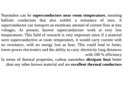
Andrew Turner 4252015 Abstract Carbon nanotubes are small tubes of carbon fiber that are prized for their electrical mechanical and thermal properties making them ideal for a variety of applications CNTs small size and thermal properties make them ideal for future transistor and interco ID: 775042

carbon nanotubes sensors nanotube carbon nanotubes sensors nanotube properties transistors www youtube production semiconductor cnt https photo applications vol

Share:

Link:

Embed:

Download Presentation from below link

Download Presentation The PPT/PDF document " Carbon Nanotubes and Related; Devices..." is the property of its rightful owner. Permission is granted to download and print the materials on this web site for personal, non-commercial use only, and to display it on your personal computer provided you do not modify the materials and that you retain all copyright notices contained in the materials. By downloading content from our website, you accept the terms of this agreement.


Presentation Transcript

Slide1

Carbon Nanotubes and Related; Devices and Applications

Andrew Turner 4/25/2015

Slide2

Abstract

Carbon

nanotubes

are small tubes of carbon fiber that are prized for their electrical, mechanical and thermal properties making them ideal for a variety of applications. CNTs small size and thermal properties make them ideal for future transistor and interconnect production providing a solution to the problem of Moore’s Law. In addition, CNT’s mechanical properties can be tied in with their electrical properties to produce a variety of sensors and related devices.

Slide3

Key Terms

CNT – Carbon

nanotube

SWNT – Single walled carbon

nanotube

MWNT –

Multiwalled

carbon

nanotube

Slide4

Outline and Introduction

HistoryCharacteristicsProductionApplications

Slide5

Questions

What are carbon

nanotubes

?

What determines if a

nanotube

has metallic or semiconductor properties?

What must we do in order to use carbon

nanotubes

in gas sensors?

What are some unique properties of carbon

nanotubes

?

What is the major drawback for the use of carbon

nanotubes

in transistors?

Slide6

History and Background

First discovered by Sumio Iijma in 1991 while looking at soot from a Fullerene experiment.Sumio Iijma has received several honors and awards including the Kavli prize.

Slide7

Characteristics

Electrical conductivity is determined by how the tubes are rolled.The armchair configuration is used to create metallic tubes.The zigzag method can be used for either metallic or semiconducting tubes.

Slide8

Characteristics

Thermal conductivity along tube axis is twice that of diamond.High current densities exceeding 1010 A/cm2.

Slide9

Production

Carbon

nanotubes

are created using single layers of graphite rolled up to form diameters of 1 to 100nm and up to millimeters in length.

Arc discharge method using electrodes

CVD – Chemical Vapor Deposition

L

aser induced traces of different types on catalyst metals

Slide10

Production

Chemical vapor deposition (CVD) is then used to grow the fibers in a catalyst containing gas with temperatures between 300 and 1150 degrees C.

The fibers are collected from the deposition system and are placed in a solvent.

The drying leaves the

nanotubes

in randomly distributed places.

Slide11

Production

The lower temperatures in the 300 to 1150 degree C range are used for multi-walled carbon

nanotube

production.

The higher temperatures in the 300 to 1150 degree C range are used for single-walled carbon

nanotube

production. Single walled carbon

nanotubes

are desired for semiconductor use.

Slide12

Applications

InterconnectsTransistorsSensorsEnergy storage

Slide13

Use in Interconnects

The use of carbon

nanotubes

in place of traditional polycrystalline interconnects allows for no

ohmic

scattering due to loss.

Decreased signal delay

Remember it is not always the interconnects for the delay. Devices themselves could cause the greatest delay.

Since carbon

nanotubes

have an extremely high current density they are resistant to current crowding.

Slide14

Use in Transistors

Switching behavior first observed in 1998 where the conductivity was observed to be modulated by about five orders of magnitude

CMOS device created when a section of a

nanotube

was doped using potassium thus reversing its conductivity.

The CNTFET outperforms the prospective Si-MOSFET when using

Guo’s

theory.

Slide15

Use in Transistors

Guo’s theory showing predicted values for MOSFETs in 2016

Slide16

Use in Transistors

It is much easier to implement vertical transistor packing because source and drain areas can be arranged vertically.

Reproducibility is difficult

Difficulty in building up for carbon

nanotube

devices as opposed to the building down of silicon based devices.

Slide17

Use in Transistors

Slide18

Use in Transistors

Cedric (Stanford)

Slide19

Use in Sensors

Can be used as environmental sensors because they can change density and conductance properties depending on what they come into contact with

Ammonia and Nitrogen Dioxide Sensors

Hydrogen and Methane Sensors

Sulfur Dioxide and Hydrogen Sulfide Sensors

Carbon Monoxide Sensors

O2 sensors

Pressure Sensors

Slide20

Use in Sensors

Pressure sensors for robotics and medical field (Stanford)Variable capacitance and material elasticity

Slide21

Other Applications

Battery Technology (Stanford)Sacha (Stanford)Conductive PastesThermal clothing sensors for firefighters

Slide22

Summary and Conclusions

Scatter free current transport allowing high current densities and improved signal delays in transistors.

Smaller feature size along with the ability to provide three dimensional stacking by implementing vertical gates and drains in transistors.

Doping or coating allows for a variety of uses in gas sensor applications.

Thin conductive layers can be produced for use in battery technology and pressure sensing.

Slide23

References

Hoenlein

, W.;

Kreupl

, F.;

Duesberg

, G.S.; Graham, A.P.;

Liebau

, M.; Seidel, R.V.; Unger, E., "Carbon

nanotube

applications in microelectronics,"

Components and Packaging Technologies, IEEE Transactions on

, vol.27, no.4, pp.629,634, Dec. 2004

^^^ Semiconductor characteristic charts for CNTs and Image of CNT

Yonggang

Zou

;

Guojun

Liu; Lin Li;

Zhanguo

Li; Mei Li, "Carbon

nanotubes

and thermal properties,"

Laser Physics and Laser Technologies (RCSLPLT) and 2010 Academic Symposium on Optoelectronics Technology (ASOT), 2010 10th Russian-Chinese Symposium on

, vol., no., pp.72,75, July 28 2010-Aug. 1 2010

Anas

, N.S., "Carbon

Nanotube

as a basic material for Sensors: A review,"

Nanoscience

, Engineering and Technology (ICONSET), 2011 International Conference on

, vol., no., pp.212,218, 28-30 Nov. 2011

Sukirno

;

Bisri

,

Satria

Zulkarnaen

;

Irmelia

;

Hasanah

, L.;

Suryamas

,

Adi

Bagus

;

Usman

, I.;

Mursal

, "Comparison of Electronic Transport Parameter of CNT(10,10)/CNT(17,0) and CNT(5,5)/CNT(8,0) Carbon

Nanotube

Metal-Semiconductor On-Tube

Heterojunction

,"

Semiconductor Electronics, 2006. ICSE '06. IEEE International Conference on

, vol., no., pp.267,271, Oct. 29 2006-Dec. 1 2006

Bondar

, A.M.; Bara, A.;

Patroi

, D.;

Svasta

, P.M., "Carbon

Mesophase

/Carbon

Nanotubes

Nanocomposite

- Functional Filler for Conductive Pastes,"

Polymers and Adhesives in Microelectronics and Photonics,

Polytronic

, 2005.

Polytronic

2005. 5th International Conference on

, vol., no., pp.215,218, 23-26 Oct. 2005

Aliahmad

, N.;

Agarwal

, M.;

Shrestha

, S.;

Varahramyan

, K., "Paper-Based Lithium-Ion Batteries Using Carbon

Nanotube

-Coated Wood Microfibers,"

Nanotechnology, IEEE Transactions on

, vol.12, no.3, pp.408,412, May 2013

^^^ Battery photo source

Slide24

References

https://www.youtube.com/watch?v=NUNpmzO1vJU

Pressure Sensor Photo

https://www.youtube.com/watch?v=NJHZylgWeJw

Cedric Photo

https://www.youtube.com/watch?v=nunbHKHc-LM

https://www.youtube.com/watch?v=QPTcQJPbGHw

https://www.youtube.com/watch?v=QvtakD9YYB8

Bike Photo

http://www.giant-bicycles.com/en-us/bikes/model/tcr.advanced.sl.1/18724/76095/

Arc discharge Photo

https://www.youtube.com/watch?v=yInS9hcYgSc

Sumio

Iijima

Photo

http://en.wikipedia.org/wiki/Sumio_Iijima

Slide25

Questions

What are carbon

nanotubes

?

What determines if a

nanotube

has metallic or semiconductor properties?

What must we do in order to use carbon

nanotubes

in gas sensors?

What are some unique properties of carbon

nanotubes

?

What is the major drawback for the use of carbon

nanotubes

in transistors?