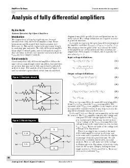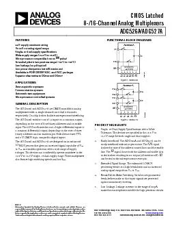
PDF-CMOS ANALOG MULTIPLEXERS/DEMULTIPLEXERS
Author : ellena-manuel | Published Date : 2017-02-23
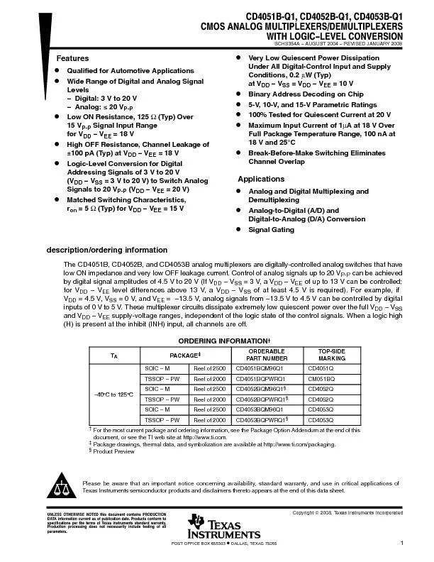
SCHS354A AUGUST 2004 REVISED JANUARY 2008 1 POST OFFICE BOX 655303 DALLAS TEXAS 75265Wide Range of Digital and Analog Signal Typ Over PACKAGE PART NUMBER TOPSIDE CD4051Q CM051BQ 40
Presentation Embed Code
Download Presentation
Download Presentation The PPT/PDF document "CMOS ANALOG MULTIPLEXERS/DEMULTIPLEXERS" is the property of its rightful owner. Permission is granted to download and print the materials on this website for personal, non-commercial use only, and to display it on your personal computer provided you do not modify the materials and that you retain all copyright notices contained in the materials. By downloading content from our website, you accept the terms of this agreement.
CMOS ANALOG MULTIPLEXERS/DEMULTIPLEXERS: Transcript
Download Rules Of Document
"CMOS ANALOG MULTIPLEXERS/DEMULTIPLEXERS"The content belongs to its owner. You may download and print it for personal use, without modification, and keep all copyright notices. By downloading, you agree to these terms.
Related Documents