PPT-The CMOS Process P. Bruschi – Microelectronic System Design
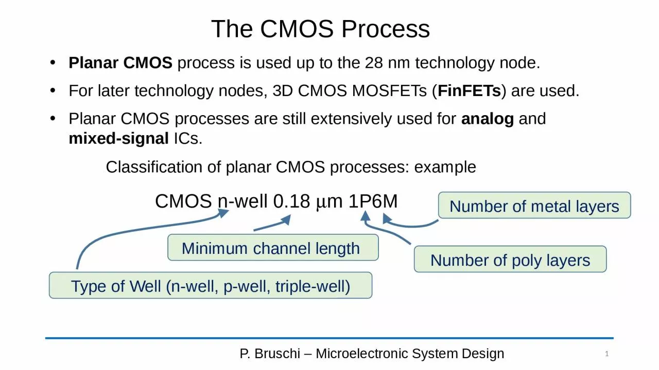
1 Planar CMOS process is used up to the 28 nm technology node For later technology nodes 3D CMOS MOSFETs FinFETs are used Planar CMOS processes are still extensively
Download Presentation
"The CMOS Process P. Bruschi – Microelectronic System Desig " is the property of its rightful owner. Permission is granted to download and print materials on this website for personal, non-commercial use only, provided you retain all copyright notices. By downloading content from our website, you accept the terms of this agreement.
Presentation Transcript
Transcript not available.