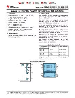
PDF-CDCLVC G GND CLKIN Y Y VDD VDD Y Y VDD GND Y Y Y GND Y Y Y VDD Y GND
Author : stefany-barnette | Published Date : 2014-11-15
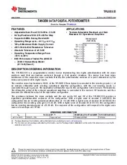
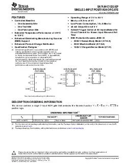
ticom SCAS895 MAY 2010 33 and 25 LVCMOS HighPerformance Clock Buffer Family Check for Samples CDCLVC11xx FEATURES Operating Temperature Range 40 to 85 HighPerformance
Presentation Embed Code
Download Presentation
Download Presentation The PPT/PDF document "CDCLVC G GND CLKIN Y Y VDD V..." is the property of its rightful owner. Permission is granted to download and print the materials on this website for personal, non-commercial use only, and to display it on your personal computer provided you do not modify the materials and that you retain all copyright notices contained in the materials. By downloading content from our website, you accept the terms of this agreement.
CDCLVC G GND CLKIN Y Y VDD VDD Y Y VDD GND Y Y Y GND Y Y Y VDD Y GND : Transcript
Download Rules Of Document
"CDCLVC G GND CLKIN Y Y VDD VDD Y Y VDD GND Y Y Y GND Y Y Y VDD Y GND "The content belongs to its owner. You may download and print it for personal use, without modification, and keep all copyright notices. By downloading, you agree to these terms.
Related Documents