PPT-1) Pin 20 (CLKIN) The
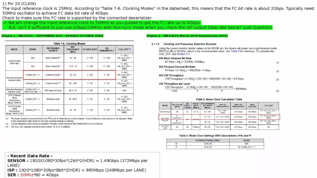
input reference clock is 25MHz According to Table 76 Clocking Modes in the datasheet this means that the FC bit rate is
Download Presentation
"1) Pin 20 (CLKIN) The" is the property of its rightful owner. Permission is granted to download and print materials on this website for personal, non-commercial use only, provided you retain all copyright notices. By downloading content from our website, you accept the terms of this agreement.
Presentation Transcript
Transcript not available.