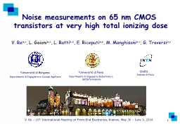
PPT-1 Noise measurements on 65 nm CMOS transistors at very high total ionizing dose
Author : mentegor | Published Date : 2020-06-23
V Re ac L Gaioni a c L Ratti bc E Riceputi ac M Manghisoni ac G Traversi ac c INFN Sezione di Pavia a Università
Presentation Embed Code
Download Presentation
Download Presentation The PPT/PDF document "1 Noise measurements on 65 nm CMOS tran..." is the property of its rightful owner. Permission is granted to download and print the materials on this website for personal, non-commercial use only, and to display it on your personal computer provided you do not modify the materials and that you retain all copyright notices contained in the materials. By downloading content from our website, you accept the terms of this agreement.
1 Noise measurements on 65 nm CMOS transistors at very high total ionizing dose: Transcript
V Re ac L Gaioni a c L Ratti bc E Riceputi ac M Manghisoni ac G Traversi ac c INFN Sezione di Pavia a Università. We build skills and con64257dence every time we sell a box We build skills and con64257dence every time we sell a box We build skills and con64257dence every time we sell a box Tell your friends to 64257nd their favorite cookies at girlscoutcookieso Module #6 – Combinational Logic. Agenda. Combinational Logic. - n-Input Gates & Equivalent Inverter. - AOI/OAI Logic Synthesis. - Transmission Gates. - Layout of Complex Logic . Announcements. M. Iuzzolino. a. , A. Tozzi. a. , N. Sanna. a. , E. Oliva. a. The outcome of Project T-REX – Sexten (BZ), 20-23/07/2015. Marcella . Iuzzolino. . Grant . holder. @ INAF - Astrophysical Observatory of Florence. Tony Affolder. University of Liverpool. LOI Costings. The core costings of the strips for the LOI was done in three parts:. In my spread sheet, I was able to cost:. All components of the stave/petals and off-detector power supplies (LV and HV). Department of Risk Management and Safety. Machine Produced. Radiation Safety. Training. University of Notre Dame. Risk Management and Safety. Radiation Safety. Overview. Ionizing Radiation. Sources. Effects. Applications. Artificially produced radioisotopes find many uses in agriculture, industry, medicine, forensic science, and scientific research.. The first practical application though of radioactivity was done by George de Hevesy in 1911. . Federico Faccio. 1. Outline. Radiation effects in CMOS technologies. Influence of scaling. Hardness-By-Design (HBD). Results in the 130nm generation. Results in the 90nm generation. A quick look beyond 90nm. Introduction. Gate Characteristics. Logic Families. Logic Family Characteristics. A Comparison of Logic Families. Complementary Metal Oxide Semiconductor. Transistor-Transistor Logic. Chapter 25. Introduction. Division of Environmental Hazards and Health Effects National Center for Environmental Health. Centers for Disease Control and Prevention (Atlanta, GA). Surveillance Using NPDS and . Radiation-related . a brief overview. Montek Singh. Feb . {7. , 12}. , 2018. Transistors as switches. At an abstract level, transistors are merely switches. 3-ported voltage-controlled switch. n-type: conduct when control input is 1. Richard Bates & . Dima. . Maneuski. Contents. Motivation for hybrid CMOS. Assembly. 10/03/16. R. Bates. 2. CMOS designs. Depleted Monolithic Active Pixel Sensor. HR-material (charge collection by drift). Number 23 1995sEverywRogkhardtsEverywRogkhardtadiationsunlightavesaysinfrared radiationainbowewiveays adiationwarimitivhnologicaldeartiadiationopagawavticlesopagaavselvessucsoundrradioactivitySucchar Radiation refers to the process that is concerned with the passage of energy between places through space. . It is the radiation generated by sun that . regulates the temperature of earth. . . CLASSIFICATION OF RADIATION: ionizing or non-ionizing types. . 1. Planar CMOS. process is used up to the 28 nm technology node. . For later technology nodes, 3D CMOS MOSFETs (. FinFETs. ) are used. . Planar CMOS processes are still extensively used for . analog.
Download Document
Here is the link to download the presentation.
"1 Noise measurements on 65 nm CMOS transistors at very high total ionizing dose"The content belongs to its owner. You may download and print it for personal use, without modification, and keep all copyright notices. By downloading, you agree to these terms.
Related Documents