PDF-Flash Erasable,Reprogrammable CMOS PAL
PALCE22V10
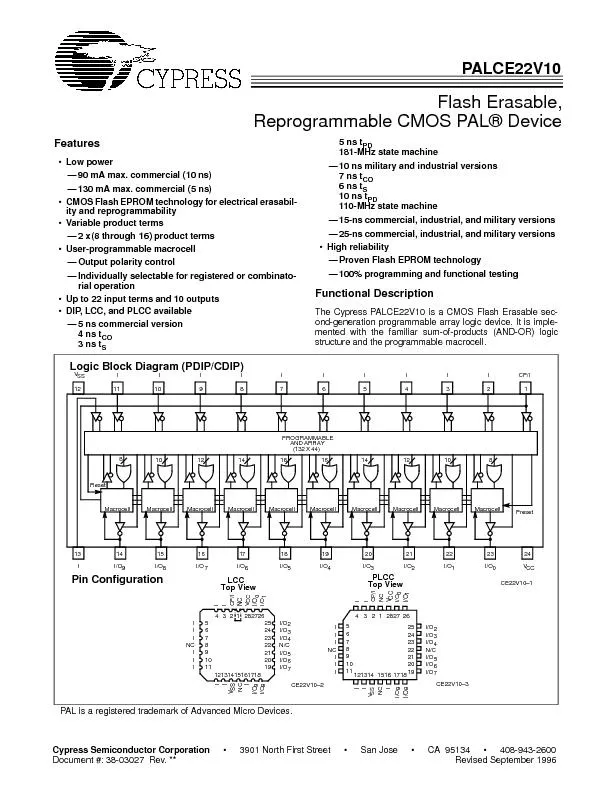
CypressSemiconductorCorporation3901NorthFirstStreetSanJoseCA 951344089432600Document 3803027 Rev Revised September 199622V10FeaturesLow power
Download Presentation
"Flash Erasable,Reprogrammable CMOS PAL" is the property of its rightful owner. Permission is granted to download and print materials on this website for personal, non-commercial use only, provided you retain all copyright notices. By downloading content from our website, you accept the terms of this agreement.
Presentation Transcript
Transcript not available.