/
Invited PaperDiazo dyeattached electrooptical polymer and its applica Invited PaperDiazo dyeattached electrooptical polymer and its applica

Invited PaperDiazo dyeattached electrooptical polymer and its applica - PDF document

hazel
hazel . @hazel
Follow
344 views
Uploaded On 2021-08-17

Invited PaperDiazo dyeattached electrooptical polymer and its applica - PPT Presentation

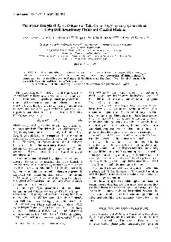
2 MATERIAL21 Polymer synthesisThe polymer studied is based on the structure shown in Fig 1 whichis called hereafter 3RDCVXY It is now wellunderstood that for an organic molecule to possess large secon ID: 864876

optical polymer loss waveguide polymer optical waveguide loss 3rdcvxy film chromophore electro light layer fig field vol cladding core

Share:

Link:

Embed:

Download Presentation from below link

Download Pdf The PPT/PDF document "Invited PaperDiazo dyeattached electroop..." is the property of its rightful owner. Permission is granted to download and print the materials on this web site for personal, non-commercial use only, and to display it on your personal computer provided you do not modify the materials and that you retain all copyright notices contained in the materials. By downloading content from our website, you accept the terms of this agreement.


Presentation Transcript

1 Invited PaperDiazo dyeattached electro-o
Invited PaperDiazo dyeattached electro-optical polymer and its applications to waveguide devices and electro-opücal samplingMichiyuki Amano, Makoto Hikita, Yoshito Shuto, Toshio Watanabe and Satoru TomaruNTI'Opto-elecironicsLaboratories, Nippon Telegraph and Telephone Corporation, Tokai, Ibaraki-Ken, 3 19-11 ,JapanMakoto Yaita and Tadao NagatsumaNTT LSI Laboratories, Nippon Telegraph and Telephone Corporation, Atsugi-Shi, Kanagawa-Ken, 243-01, JapanABSTRACTAn electro-optical polymer was synthesized where a diazo dye with a dicyanovinyl group as an electron acceptor and adiethylamino group as a donor is attached to the polymer chain. The electro-optical coefficient (r) reached 30 pm/V. It wasfound that the edge absorption of the chromophore caused a loss increase in the near infrared region, which indicates that theincrease in the r vaJu leads to a propagation loss increase in the material. The loss is around 1 .0 dB/cm in a single-modewaveguide fabricateU by using oxygen reactive ion etching. The polymer waveguide is applied to two types of device, a Mach-Zehnder optical modulator and a vertically stacked directional coupler, which both achieve electro-optical modulation. Asanother application, eleciro-optical measurement of an electric field in a high-speed circuit device is demonstrated, where thepolymer is processed into a chip film probe and patched to an integrated circuit, thus enabling the electric signal to be detected.1. INTRODUCTIONThere has been significant progress in the nonlinear optical application of polymeric materials. These polymericsystems consist of a matrix polymer with a nonlinear optical chromophore as a guest or attached as a side chain. The nature ofthe chromophore determines the nonlinear optical properties, and considerable effort has been made to design and synthesize newchromophores with increased nonlinear coefficients.'These nonlinear optical polymers have the potential for use in fabricating low-switching-voltage and high-speed eleciro-optical devices.2' 3 And they can be cost-effectively processed and formed into thin films with good optical quality, whichmakes them particularly useful for designing a variety of electro-optical (EO) waveguide devices.4' 5Theseadvantages havebeen demonstrated by recent research. More recently, efforts have been made to fulfill the requirements for successful deviceapplication.6' 7 8 These are long term temporal stability at elevated temperatures as well as at high optical power and lowpropagation loss at the operation wavelength. Although many kinds of organic chromophore with great potential have alreadybeen developed for EO polymers," 9 10 only one or two kinds of well-known chromophore, i. e., di

2 sperse red 1 andd*ethylaminonitrostilben
sperse red 1 andd*ethylaminonitrostilbene, have been applied in reported EO devices. This is because the newly developed chromophores aredifficult in terms of film preparation with good optical quality and large scale synthesis. Therefore, there have been fewattempts to use such chromophores in waveguide applications.On the other hand, the above advantages of EO polymers can be utilized in fields other than waveguide deviceapplication. Recently, there have been several reports on a new application of EO polymers, that is, the electro-opticalsampling (EOS) technique, where EO polymer films can be used as probes. Their electro-optical response, permittivity, cost-effectiveness and processability are superior to those of inorganic EO materials, and these advantages offer the possibility ofobtaining polymer sensors for high speed electrical signals at a low cost.This paper describes the characterization of a diazo dye attached EO polymer, which we have been developing in recentyears, with a view to waveguide application and also mentions the fabrication of waveguicle devices including an EO waveguidewith a novel stacked structure. As another application, EOS measurement is demonstrated using a polymer film chip probe forelectrical signal detection in an integrated circuit.68/ SP1E Vol. 2143O-8194-1438-7/94/$6.OO 2. MATERIAL2.1. Polymer synthesisThe polymer studied is based on the structure shown in Fig. 1 ,whichis called hereafter 3RDCVXY. It is now wellunderstood that for an organic molecule to possess large second-order opticai nonlinearity, the molecule needs to contain a longIt-conjugatedsystem where the ic-electrons are delocalized over the length of the molecule, with one end of the moleculeattached to an electron donor group and the other end attached to an electron acceptor group. Pendant diazo dye contains adicyanovinyl group as an electron acceptor, a diethylamino group as an electron donor and a three benzene rings connected withazo groups, which form a long ic-conjugated system. Although three ring benzenoid molecules with a strong electron donor andacceptor generally have very poor solubility, the attached two methyl groups are expected to increase the solubility. Regardingthe second-order nonlinear optical parameters and other properties, see reference 9.3RDCVXY was synthesized as shown schematically in Fig. 2. The synthetic route includes a reported procedure wherea polymer coupler and a diazonium salt undergo a diazonium coupling reti1 The polymer coupler was obtained by radicalcopolymenzation of (N-ethyl)anilinoethyl methacrylate and methyl methacrylate using 2, 2'-azobisisobutyronitrile as aninitiator. The molecular weight was properly adjusted by add

3 ing a chain transfer agent. The copolyme
ing a chain transfer agent. The copolymer was dissolved in amixture of acetic acid and propionic acid. The diazonium salt solution in acetic acid of 4-(4-(dicyanovinyl)phenylazo)-3,5-xylidine was then added to the polymer solution dropwise. Sodium acetate was then added and the reaction mixture was stirredvigorously until the color turned deep red. The reaction temperature was maintained at less than 15 'C. The polymer wasdissolved in acetic acid and purified by reprecipitation from methanol and by removing ionic impurities by washing with water.The polymer was then dried. The purified polymer was dissolved in chlorobenzene and the solution was roughly filtered toremove insoluble residue and then carefully filtered in a clean room using a polymer membrane filter with the pore size of lessthan 1 .0 tm to provide a solution for spincoating. The other synthesis procedures were as follows;(N-ethyl)anilinoethyl methacrylate was obtained by the reaction of (N-ethyl)anilinoethanol and methacryloyl chloride inthe presence of triethylamine at room temperature. The diazonium salt of 4-(4-(dicyanovinyl)phenylazo)-3,5-.xylidine wasobtained by adding a solution of sodium nitrite in sulfuric acid to the acetic acid solution. The reaction temperature was keptbelow 5°C.4-(4-(dicyanovinyl)phenylazo)-3,5-xylidine was synthesized from 3, 5-xylidine and clicyanovinylaniine12 using thesame method.3RDCVXY with the main chain hydrogens partly substituted by deuterium atoms was also synthesized by using theprocedures described above. Here, 68 -77 % ofthe aikyl hydrogen atoms were substituted by deuterium. This polymer isexpected to show a lower absorption loss than the unsubstituted one at wavelengths in the near infrared (IR) region.2.2. EO coefficientThe EO coefficient was evaluated by the reflection technique reported by Teng and Man.13 The essence of this methodis to measure the change in phase of the light reflected from a poled polymer film whose top surface is covered with atransparent electrode of indium tin oxide (ITO) and whose bottom surface is a gold layer. Here, the 3RDCVXY film was spin-coated on a silicon wafer coated with a thick evaporated gold film. It was poled by applying an electric field using a metal blockelectrode with the gold film grounded, at a temperature of 140 'C. The poled film was then covered with an ITO glass. Thesample was irradiated with 1.31 pnilightfrom a semiconductor laser diode (LD), which was polarized and rotated at 45°togiveequal amounts of s and p components. The reflected beam was allowed to propagate through a ir/4 plate, an analyzer and into adetector. The modulation in the beam was measured using a lock-in amplifier. By adjusting the phase

4 retardation to ir/2 formaximum sensitivi
retardation to ir/2 formaximum sensitivity, the modulating electric field caused a phase change resulting in a change in the intensity of the reflectedlight from which the change in the refractive index was calculated. The EO coefficient was then determined from therelationship between the electric field strength and the refractive index change. Although the EO coefficient of an EO polymer isknown to be proportional to the poling field and the content of the nonlinear optical chromophore, the value of 3RDCVXY waslimited by the dielectric breakdown voltage and the chromophore content at which polymer film with good optical quality can beformed (less than 15 mol%). The coefficients were 20 pm/V and 30 pm/V at chromophore concentrations of 10 mol% and 15mol%, respectively. The applied electric field in each case was 80 % of the dielectric breakdown voltage. These are comparableto the LiNbO3 value (31 pm/V), and hence are acceptable for prototype device application. To obtain a higher EO coefficient,SPIEVol. 2143 /69 �improvements are needed in the polymer characteristics, that is, both a high durability for dielectric breakdown ( 150 V/gm)�and a good optical quality of film must be achieved even at a high chromophore concentration ( l5mol%).2.3. Loss characterizationPropagation loss is one of the most important performance characteristics in optical components. The disadvantage ofpolymer waveguides is the intrinsic absorption due to vibrational overtones of C-H, N-H and 0-H bonds in thetelecommunication wavelength, that is, in the near IR region. Recently, there have been attempts to remove or substitute thesebonds and thus directly reduce the propagation loss of the waveguides.14' 15 For electro-optical polymers, however, it ispossible for edge absorption caused by the electronic transition of the charge transfer band of the nonlinear optical chromophoreto be superimposed on the vibrational absorption. Here, the propagation losses in slab waveguides of both 3RDCVXY andpartly deuterated 3RDCVXY were measured. Their intrinsic absorptions were also characterized.Films approximately 3 -5 jtmthick were formed on glass substrates. LD-pumped YAG laser light at 1.32 p.m wasthen launched into the film and the intensity of the scattered light along the streak was measured with a charge coupled device(CCD) camera. For 3RDCVXY, the waveguide propagalion losses were estimated to be 0.7 dB/cm at a chromophore content of10 mol%, and Li dB/cm at 15 mol%. On the other hand, the losses of the partly deuterated 3RDCVXY were 0.5dR/cmand0.8 dB/cm for a chromophore content of 10 mol% and 15mol%,respectively. The lower loss in the deuterated 3RDCVXY canbe attributed to the sm

5 aller absorption of the vibrational over
aller absorption of the vibrational overtone of C-H, because the loss differences are 0.2 -0.3dB/cm andthe these are comparable to the difference value between PMIIIA and deuterated one (around 0.2 dB/cm). The absolute lossvalues obtained here are much higher than that of PMMA (0.3 dB/cm or less), and therefore the presence of the chromophoreseems to lead to their intrinsic absorption.In order to understand the origin of these losses, transmission spectroscopy was used to measure the intrinsicabsorption spectrum. The spectrum can be characterized by transmission spectroscopy or by photothermal deflectionspectroscopy.6 Here, the former method was used because it is the most direct and easiest approach. Films with a thickness ofseveral tens of microns were formed on glass substrates and their optical absorptions were measured in a spectrophotometer(JASCO, MAC-i). The measured spectra are shown in Fig. 3, where the non-functionalized polymer means the polymercoupler mentioned in 2.1 (copolymer of (N-ethyl)aniinoethyl methacrylate and methyl methacrylate). The wavelength regionwas between 0.7 -1.6 jim. The propagation losses and zero levels of the ordinate in Fig. 3 (a) were determined by measuringsamples with various thicknesses. The important disadvantage of this method is that truly quantitative loss can not becharacterized for the thin film samples obtained here. Thick films over 50mm,which are very hard to prepare and which requirea significant amount of material, are needed for this purpose. Although the accuracy with which the propagation loss isdetermined is then less precise where the value is small (at around 1.3 mi),aqualitative understanding of the loss mechanism ispossible. Figure 3 (a) shows that the loss increases with an increase in the chromophore ratio over the wavelength region ofaround 1.3 im and below and this explains the loss results in the slab waveguides. The loss increment is larger at shorterwavelengths and this is proved from Fig. 3 (b) to be caused by an edge absorption resulting from the electronic transition of thecharge transfer band of the chromophore, where the tailing changes exponentially and no chromophore aggregation is detected.Therefore the scattering loss appears small compared to the absorption loss. This result indicates that the increase in the E0coefficient leads to a propagation loss increase due to chromophore absorption in the 1.3 jim wavelength region, and this factshould be taken into consideration when designing waveguide devices. Figure 3 (c) shows the loss spectrum of the partlydeuterated 3RDCVXY. This spectrum also corresponds to the result of the loss decrease in the slab waveguide.3. OPTICAL WAVEGUIDE DEVICESThe p

6 rocessing of polymers into thin layers i
rocessing of polymers into thin layers is well established and cost-effective. This approach includes spin coating,dip coating and bar coating. These techniques result in smooth polymer surfaces which can be patterned to micron size withconventional photolithographic or photochemical methods. These polymer technologies provide a high degree of flexibility inwaveguide design and a means for cost-effective manufacturing on a large scale. Recently, there have been several reports onMach-Zehnder interferometers using E0 polymer terial3 and a potential 3-dimensional integrated polymer waveguide wasalso reported16 where the two stacked levels are independently operated. These reports stress the potential of polymers forintegrated optics applications. Here, an EO Mach-Zehnder modulator using 3RDCVXY is described along with waveguidefabrication. A vertically stacked E0 coupler is also proposed and its potential applications are discussed.3.1. Waveguide fabrication70 ISPIE Vol. 2143 Channel waveguides were processed by using the following etching technique. First, UV curable epoxy resin for theunder cladding layer was coated on a silicon wafer and cured by UV radiation. The UV resin had been purified by filtering itusing a membrane filter with a pore size of 0.5jtm.The refractive index of the UV resin was subjected to precise control in theI .530to1 .550rangeat a wavelength of 1 .3 1 p.m to satisfy the requirement for a single-mode waveguide. This was followed bythe spincoating the underciadding layer with partly deuterated 3RDCVXY. The refractive index of 3RDCVXY was about 1 .54at1 .3 1 jim, and the relative index difference, n, between the core and the cladding polymer was between 0.2 -0.6%at 1 .3 1 tm.The film thickness was 5p.mfor the core and 10 pm for the cladding layer. Next the channel waveguide pattern mask wasfabricated using conventional photolithography. The core ridges were then formed by oxygen reactive ion etching (02 RIE)until the under cladding layer surface was exposed. Subsequently the mask was removed. Figure 4 shows a rectangular coreridge of EO polymer formed by O RIE and photolithography. Smooth waveguide walls and a flat top surface are confirmed.The size was controlled by these techniques with high accuracy. Finally, the core ridge was covered with a cladding layer byspincoating. The subsequent deposition of polymer to form the cladding layer resulted in nearly perfect core-cladding interfaces.The near-field mode pattern and optical intensity distribution are shown in Fig 5.Thisfigure confirms the single modeoperation of the fabricated waveguide.Loss measurements were performed for straight waveguides using a 1.3 1 p.m wavelength light source. A sin

7 gle modefiber with a mode-field diameter
gle modefiber with a mode-field diameter of 9.5p.mand a multi mode fiber were used as input and output fibers, respectively. The 1.31im wavelength output from a laser diode was first launched into the input fiber. The input and output fibers were then buttedagainst the waveguide and precisely aligned. Silicone oil was used to reduce the mismatch between the waveguides and fibers.The propagation loss was determined by the cut-back method, the loss was calculated to be 1.0 -1.1dB/cm from the slope ofthe curve as a function of waveguide length when the chromophore concentration was 10 -15 mol%.3.2. Mach-Zehnder modulatorA Mach-Zehnder modulator using the partly deuterated 3RDCVXY is schematically shown in Fig. 6. The deviceconsists of a Mach-Zehnder optical waveguide and a gold microstrip electrode on one of the arms. The waveguide fabricationfollowed the procedures described above. The microstrip electrode was 15 mm long and the core was 4.0 jim wide and 2.5p.mhigh. The EO polymer was poled by applying an electric field between the microstrip electrode and the lower gold electrode.The electro-optical modulation was tested using a 1.32 p.m LD-pumped YAG laser. TM polarized laser light was coupled intothe modulator from a polarization-maintaining optical fiber. The modulation light was also coupled into the output optical fiberpigtailed to a Ge photodiode detector. The intensity response was displayed on a processing oscilloscope after the signal hadbeen averaged 100 times. Figure 7 is the measured response of the modulator to a triangular waveform. The efficiency of theoptical modulation was evaluated by using the half wave voltage (Vir), which is defined as voltage necessary to shift the incidentlight phase of it.Atentative result was a Vic of 29 V for a triangular wave of 40 Vp-p and 10 kHz. The 33 of the waveguidewas calculated from the Vic by the following equation,33 =?dI(N3LVic).where d is the spacing between electrodes, X is the incident light wavelength, N is the effective refractive index in thewaveguide and L is the length of the microstrip electrode. 33 was then determined as 9 pm/V. The value does not reach theinherent EO coefficient (30 pm/V), which indicates that improvements will be needed in the waveguide poling technique andalso in the cladding materials. No change was observed in the modulated signal for more than 150 hours when the modulatorwas continuously operated using a CW laser with a power of 1.5 mW at a modulation frequency of 10 MHz and also at 100MHz. This suggests that no damage occurs in the chromophore for an extended period of continuous use when a widelydistributed 1 mW light source is used.3.3. Vertically-stacked waveguide device'7Whe

8 n fabricating a vertically stacked coupl
n fabricating a vertically stacked coupler as shown schematically in Fig. 8, it is of great importance to control thewaveguide spacing between the upper and lower cores. One core is made of partly deuterated 3RDCVXY and the other of a UVcurable epoxy resin. Therefore, a process for waveguide stacking was developed where the spacing is precisely controlled. First,the under cladding and the lower core layers were spincoated on a silicon substrate. The lower core ridge was made according tothe process outlined in 3.1, then covered with a middle cladding layer by spin coating. UV curable epoxy resin was also chosenSPIEVol. 2143 / 71 for the cladding polymer. The thickness of the middle cladding layer was precisely controlled by the spinning speed and thespinning time and the top surface was confirmed to be flat enough for stacking the upper waveguide layer. The refractive indexof 3RDCVXY was 1.54 at 1.31 im and the relative index difference, z.n, between the core and the cladding polymer at 1.31 .tmwas 0.2 -0.6% as the single-mode conditions were satisfied. The same process was then repeated for the upper core and theupper cladding layer. The distance between cores was controlled at 3.5jtm.The core size of the coupler was 3.5x5j.tm2.A1 .3 1 p.m laser light was input through a single-mode fiber with a spot size of 8 j.tm which was butt-jointed to the lowerwaveguide. The near field mode patterns at a cross section of the coupler interaction region and at the output are also shown inFig. 9. These results clearly prove that the vertically stacked coupler operates as well as conventional in-plane couplers. Asshown above, different channel paths between the lower and the upper channels can be designed independently. This waveguidefabrication technique therefore has an advantage compared with a conventional technique such as photobleaching, and illustratesthe potential for application to three dimensional switching devices where vertical couplers and switches have been attractingconsiderable attention as key elemen&821The optical intensity modulation was also measured in the device shown in Fig. 8. When an electric field modulationis applied between the electrodes, only the refractive index of the EO polymer is changed. Before the measurement, poling wascarried out at 140 'C with an applied voltage of 500 V. The total polymer thickness between the electrodes was about 40 pm.The interaction length of the coupler was approximately 6 mm. A 1 .31 p.m light was input through the polarization-maintaining optical fiber butt-joined to the lower waveguide. When the voltage was applied between the electrodes, the output-light intensity was detected by a Ge photodiode detector through t

9 he butt-jointed fiber. The intensity res
he butt-jointed fiber. The intensity responses of both theupper and lower cores were displayed on a processing oscilloscope after the signal had been averaged 100 times. The modulationfrequency was 10 kHz. The dependence of the modulation response on the applied voltage was clearly observed. However, thetotal light intensity throughout the waveguide changed less than 10%. As with Mach-Zehnder modulator, the estimatedvalue was smaller than the intrinsic potential of the polymer value (less than 5pm/V).This implies that the poling conditionswere not optimized, which is a problem that remains to be dealt with.4. POLYMER PATCH SENSOR FOR EO SAMPLINGEOS is based on the high-speed interaction between the electric field and light in an electro-optical material, and is aproven technique for the non-destructive measurement of very high-speed electhcal signals. This technique can be applied to thediagnosis of electrical circuits such as integrated circuits (ICs), multichip modules or printed circuit boards by sampling anoverlying eleciro-optical layer. In previously used measuring systems, the electro-optical media were inorganic crystals, i. e.GaAs, LiNbO3 and LiTaO3. Recently, several studies have been published on EOS with poled polymer films.22 26 This isbecause electro-optical polymer materials have an ultrafast electro-optical response and low permittivity, which results in lowcircuit loading even if the polymer film is in direct contact with the circuit under test. These include the first experiment on apolymer patch sensor22, the detection of microwave signals at frequencies up to 20 GHz using the interferometric technique23,the measurement of subpicosecond response time using a femtosecond dye laser24, and a sampling technique using asemiconductor laser diode25 as well as theoretical evaluation26. Here, we demonstrate EOS with a polymer patch sensor madeof 3RDCVXY which gives an internal waveform of an analog IC using a semiconductor laser diode.4.1.Patchsensor preparationAlthough a low propagation loss is required for EO waveguide devices as explained in 2.3, surface optical quality ismore important for patch sensors, because the interaction length is several tens of microns at most. Therefore, our focus was onimprovement of the film quality in the sensor development. The patch sensor was prepared as follows. A 3RDCVXY solution,which was prepared according to the procedure described in 2. 1 ,wascast on a silicon wafer to give a film with a thickness of 15-20pm. This was followed by overcoating with a flexible and transparent polymer as a supportive layer to the 3RDCVXYfilm. A metal electrode was set on the two-layered film which was then poled at around 140 °C by a

10 pplying an electric fieldwith the silico
pplying an electric fieldwith the silicon wafer grounded. After cooling, the two-layered film was separated from the silicon wafer to give a free-standingfilm with an good optical quality surface. The film was cut into patch sensors 1 mm x 1 mm in size. All the proceduresmentioned here were undertaken in a clean room. The EO coefficient of the sensors was estimated to be 15 -20 pm/V.4.2. EOS exprimnt72ISPIE Vol. 2143 The patch sensor was directly attached to a 10 0Hz amplifier IC chip27 by commercial optical adhesive with arefractive index almost the same as that of the polymer. The adhesive layer was less than 1 jtm thick. The sensing systemconfiguration is shown in Fig. 10. The probing laser beam is incident on the side of the coating film at an angle of 9. Thebeam propagates through the coating film and the EO polymer layer, and then is reflected by the surface of the metal line.Some change in polarization of the beam is induced by the longitudinal component of the electric field on the metal line. Thelaser source was a 1 .3 .tm InGaAsP/lnP DFB semiconductor laser diode, which was gain-switched to generate an opticai pulsewith a width of 20 p5 FW.HM and an average power as low as 100 tW at a repetition rate of 100 MHz. The opticalbeam wascollimated to a spot of about 10 mm in diameter to obtain a near-diffraction-limited spot of less than 2.5 jtm in diameter afterpassing through the object lens. The polarization of the probe beam was set at 45 °tothe incident plane. The incident anglewas 50° The reflected beam propagated through another objective lens, a waveplate, a Wollaston prism, and into a pair ofphotoconductors. The detachable mirror was used only in the process of directing the probe beam onto the circuit under test, andwas removed during the measurement.Figure 1 1 shows a photograph of the measured IC chip, where (a) and (b) are the input and output ends of the IC line,respectively. The electrical signals there were detected by EOS as shown in Fig. 12. The signal frequency was 80Hz. Thedetected amplitudes of the input and output signals were 3OmVp-p and 320 mVp-p, respectively, which indicates a gain of about20dB. These values are in good agreement with the result detected by a network analyzer.2° The noise level shown in thefigure was less than 1 mY, and in practice the signal is analyzed up to lOmVp-p. This result implies that the patch sensor madeof 3RDCVXY is applicable to the diagnosis of analog ICs in spite of the small signal level.5. CONCLUSIONSAn electro-optical polymer in which a diazo dye with a dicyanovinyl group as an electron acceptor and a diethylaminogroup as a donor is attached to the polymer chain (3RDCVXY) exhibits an electro-optical c

11 oefficient of 30 pmfV. The edgeabsorptio
oefficient of 30 pmfV. The edgeabsorption of the chromophore causes the propagation loss increment to around 1 .3 rim, which indicates that a loss increaseshould be taken into consideration when designing waveguide devices. The waveguide loss can be reduced by 0.2 -0.3dB/cmusing a partly deuterated 3RDCVXY. The single-mode waveguide can be successfully fabricated by using an oxygen reactiveion etching process, with the loss of 0.9 -I.1dB/cm when varying the chromophore content. The 3RDCVXY waveguide isapplied to two types of device, a Mach-Zehnder optical modulator and a vertically stacked directional coupler, which both achieveelectro-optical modulation. The fabrication technique for the stacked device is a step towards the fabrication of 3-dimensionaloptical components. Another application is to use the chip film of the EO polymer for the electro-optical measurement ofelectric fields in high-speed devices and integrated circuits.6. ACKNOWLEDGEMENTSWe would like to thank Dr. Ando for measuring the precise near-JR spectrum, Dr. Kaino for the polymer synthesis, Dr.Sugii and Dr. Kozawaguchi for their continuous encouragement.7. REFERENCES1 .K.D. Singer, J. E. Sohn, L. A .King and H. M. Gordon, "Second-order nonlinear-optical properties of donor- andacceptor-substituted aromatic compounds", J. Opt. Soc. Am. B, Vol. 6, No. 7, pp. 1339 -1350,1989.2. D. G. Girton, S. L. Kwiatkowski, G. F. Lipscomb and R. S. Lytel, "20 GHz electro-optic polymer Mach-Zehndermodulator", App!. Phys. Lett., Vol. 58, No. 16, pp. 1730 -1732,1991.3. C. C. Teng, "Traveling-wave polymeric optical intensity modulator with more than 40 GHz of 3-dB electricalbandwidth", App!. Phys. Lett., Vol. 60, No. 13, pp. 1538- 1540, 1992.4. J. I. Thackara, G. F. Lipscomb, M. A. Stiller, A. J. Ticknor and R. Lytel, "Poled electro-optic waveguide formationin thin-film organic media", App!. Phys. Lett, Vol. 52, No. 13, pp. 1031 -1033,1988.5. G. R. MOhlmann, W. H. 0. Horsthius, C. P. J. M. van der Vorst, A. McDonach, M. Cope!and, C. Duchet, P.Fabre, M. B. J. Diemeer, E. S. Trommel, F. M. M. Suyten, P. Van Daele, E. Van Tomme and R. Baets, "Recentdevelopments in optically nonlinear polymers and related electro-optic devices", SPIE, Vol. 1147, pp. 245 -255,1989.6. A. Skumanich, M. Jurich and J. D. Swa!en, "Absorption and scattering in nonlinear optical polymeric systems",App!. Phys. Lett., Vol. 62, No. 5, pp. 446 -448,1993.SPIEVol. 2143/73 frLZ 7OA3IdSIfrL Z661 '061 -csi dd ' 'ON 'Ot' 'I°A "P°L (.iootij AMO13iJ SuEij 3331 'SWOISAS uouownwwoo jorido pods-qiq ioj sy puqopM jo oouuuoj.id pu uisocj, 'sv 'j pu ou 'wi 'A 'L7 66T 'SZZ - ZZZ dd ' 'ON 'D-9L IA 'UOi1OO 'SUEkL DI1 11'EpIU ouuicjod pojod ui sjus jospjo jo 2uqduis

12 joridcj, 'U1fl12E .i pu mA 9Z '66t 'SL1
joridcj, 'U1fl12E .i pu mA 9Z '66t 'SL11 - £LET'I dd '6 'ON '1 'bA 'Z id "SAqd iddy f ud '6siowAjod pod uisn 2mjdums orido-oiioojo uiix '' Pu 1!!A 'J' 'EWflSEN 'j 'cz; '1661 ':c9z - 1c9z dd 'j 'ON '6c '1°A "UO'[ 'SAq 'jdct 'siuiAod pod ondo-onoojo ,jo osuodsoi PuOoosO1uIod4 'UO1SflT 'H 'ci pu 2UEq '3 'x "H ' 'I '!P1A '1. '1 'flA& '3 'dduN ' ' 'j 'd 'PZ '1661 '1911 - 6c11 'dd 'j 'ON '6 'bA "flo,1 'SALj 'jddy 'ipui otuio pood jo &nidums 3ndo-oxp1 'Pinv 'y '[ puE WOO 'J 'ci '1pqj 'I 'f ' ' T66!'t6 - Z6 'dd ' j 'ON 'U 'bOA "fl'1 'UO1I3j3 'S2ifl3flO jO11bUI U! SJEU2IS jOUOOj JO 1UOWO1flSW ondo-oiijo ,IOj JOSUOS qod 3!UE1O1, 'OWIIS 'A PU OUEUIy 'J 'ME2Uiq ' '!A '"i 'wns1E2N 'j, ' 't661 '181 T'l - 081 11 'I 'bOA "Si(q 'jdciy 'ç 'udç ',iowAjod odo-oiiooio 2msn siij oprn2AM PO1OE1S uoiwioq qoliMs j0do pojdnoo-juonoii1, '1flWiqSOA 'A PL iqsoAoioj, 'j 'mnsj. 'S 'unAoo ' 'tz 'Z661 'zair 'Z6 I OTD '41S1TU3fl,rIS Opifl2AM IOUIXjOd ondo-oziooj IA1flIN 'qwoosdi 'j 'o pu joi' 'S 'a 'uoiq 'o 'a 'oz 't661 '8P Lt' 'cid 'ç 'ON '8Z 'bA "fl,1 'UOI13Oj '!S UO SOpU1OAN 1UUI OqIS-qIq po1,I2U! 'II3!UA4 'U1flO4''T "?l '1 'ci ssoiqm ' '61 't661 ' 8cZ1 - 9cz1 'dd ' 'bOA "un 'jouqooj 'uOloqd m 's uo OpiflOAEM 3!llS JO SIOi(EI jOjO1S OiW1 q1M siouosi uu ondo-poiiiuI14 'ou!q}j 'A P" 0lIS ') 'DjflZfl 'S '81 '661 '9t I - 191 1 'dd '6 'ON '9 'bOA "fl'TI 'S1C14d 'jdci 'iuiAjod ondo-onojo uuiothooui ojdnoo ppms JCUOUOA UI UOUEjflpOW iUSUOUI joudO, 'IqOfl2EMZO( 'H tUUIOJ, 'S '1flUUSO 'i 'OUUFT ' 'O14S 'A 'flPI!H 'N 'LI '66T 'OLO - 89O 'dd 'ti 'ON 't9 'bOA "IWl 'SAq 'iddy '1i(i,m JOjflpOW Ausuoiui iopuqo-p ououiiod piosi2i 1AIn!flw1 'AONSV 'a 'd pu 'If 'OffljOWfl 'f 'J '91 '661 'ILZ - 69Z 'dd ' 'ON '6Z 'bOA "II"J 'UO113j '1SOjUIAOd pouuonj MOU UISfl SOpIflAM j3I1do iuisisi-iq 'ssoj MO"J, 'OJOUJEUJEA 'd P !1S 'S 'OPUV 'S '2J 'I 'SI '1661 'EiI-ZPI 'dd 'SI 'ON 'U 'bOA "TiOTI 'UOI13Ob '44uiil £'J SSOJ AOj LflIM Sp!nAM IUUl 1WAbOd44 'izj 'j pim E1flUflSOA '1 'mU1LUI 'S 'P1 '0661 '9L1 - PL1 'dd 'gj 'ON '95 'bOA "U'1 'SiI4d 'iddy 'siowAjod pojod Jo IUO!OIJJ000 ondo-oziobo tfl UIiflSW IOJ nbuqo uonojjai bdwIS., "EN 'I 'H P UOJ '3 '3 'El . '8561 'SISZ 908Z 'dd 'Og 'bOA '0S 'U11D 'WV '1 '1SOURUj(UIAOUEiOUj 'IA 'flS!WP UOqmoOui( 'ioio 'j 'H UEWJJO3 'Q 'Q 'SUflE ' 'j 'UO13H ' ',I '3Sfl3Ji '3 ' 'Zl '8861 'OPSS - SESS 'dd 'ES 'bOA 'U13 'J() 'f '1sodo ,mouquou ioj sijs wn!UOz!pUozUq p1rni1sqrLs-jArnAouAo jo SUOIII pu ssqiuA 'xo ' 'j pu 'zij ' 'H 'Ufflq3 "1 'TN '11 '0661 '8t09 - i7t09 'dd 'ZI 'ON '89 'bOA "S1Id 'jdciy 'j 'iowod poqoi-oip-ozp jOAOU JO A1TJUflUOU ipio-puooo 'ouj 'j ptm ouwy 'j '01 '1661 'S61 - P81 'dd 'o9c 'bOA 3ldS 'siowAjod pojod ponuisqns-oAp-oz jOAOU UI UOIEjflOW 'ou 'j. puc oucwy 'ji 'Oiflq 'A '6 '

13 E661 'LO9Z - 509Z 'dd 'Z9 'bOA "TlO'l 'S
E661 'LO9Z - 509Z 'dd 'Z9 'bOA "TlO'l 'SAq 'jddy 'suuuijuou Jp1o-puO3os jqs IOJ siouiijod uip uiw ppuoq cjwopuEJ JO UDjUIjSSOJO J!ULILP puc 2UIjOd 0UJ1 't10MEQ "1 P M ' 'X '3 '11S 'H 'A\ "4S 'A 'UOUWJ 'N 'd '8 'E66l '9L8P - TL8P 'dd '8 'ON 'PL 'I°A "fl"J 'SCq 'jddV 'spInoAM poudo iouquou ouuAjod jo soqiodoid &njpucq itod jmndO1 'uj '3 puc UOOA 'V 'H 'rAzuoN 'V 'N 'L CH3CH3*CH2C}x(CH2—)coCO9aCH3F1cH3CH3-fcH2---c)x(cH2—.ç)1.c=oç=oa9CH3C2H4CH3COONain CH3COOH12hrs.(1) reprecipitatedwith CH3OH(2) washedwith H203RDCVXYFig. 2. Procedure for synthesizing 3RDCVXY.SPIE Vol.2143 / 75R1=C2HH(ON)2Fig. 1. Basic structure of the polymer, 3RDCVXY.++.HH3 E0Cl)Cl)0-JEaCl)Cl)0-JFig.3. Loss spectra of 3RDCVXY. (a) represents the dependence of loss on the chromophore content in the near JR region,where the solid line represents 15 mol%, the dotted line 10 mol% and the dash-dotted line represents the non-functionalizedpolymer described in the text. (b) shows the loss spectra for 3RDCVXY of the chromophore content of 10 mol% (solid line)and non-functionalized polymer (dash-dotted line) in the wavelength region of 0.7 -1.1rim. (c) represents the loss spectra of3RDCVXY (dotted line) and partly deuterated 3RDCVXY (solid line) where 77% of the C-H hydrogen atoms are deuterated. Thechromophore content is 10 mol% for both cases.76ISPIE Vol. 2143E0Cl)Cl)2O1.4Wavelength(pm)Wavelength (pm)Wavelength (am) the fabricated waveguide.EO Polymer Channel WaveguideAuEO Polymer (4 x 2.5pm)/IUV Cured Polymer\11j.tmAuSi WaferSi OxideFig. 6. Structure of the Mach-Zehnder modulator.Fig. 7. Intensity modulation response of the Mach.Zehndermodulator at 1.31 p.m.SPIE Vol. 2143 / 77Fig. 4. Scanning..electron-microscope photograph ofFig. 5.Profileof the light intensity disthbution ofthe core ridge of 3RDCVXY formed by 02 RIE.SMA ConnectorsMicrostrip Electrode (L =15mm) output lightport)outputlight(through port)Fig. 8. Schematic view of a vertically stacked coupler.(c)uppermiddlelowerSi02/Si substrateFig. 9. (a) Optical-microscope photograph of cross-sectional view using visible light. (b) Near-field pattern of the verticallystacked coupler when 1.31 mm laser is input from the lower channel waveguide. (c) Profiles of the light intensity distributionof the coupler.78ISPIE Vol. 2143Au upper electrodeground planeelectrodeinput lightcladdinglayerupper channellower channel(a)(b) poled __________________polymerl___________________Fig. 11. Photograph of a measured amplifier ICchip.IC substrateFig.10. Schematic configuration for EOSmeasurement.(a)C)0(b)Fig. 12. Measured signals of amplifier IC at input (a) and output (b) ends.SPIE Vol. 2143 / 79supportfilmIinput:::ir2TI2::TS:7I—.11output,7\J/\/\i..f3OmV300mVtIme (62.5 ps/