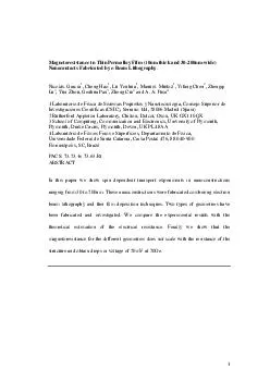
PDF-Magnetoresistance in Thin Permalloy Film nmthick and nm wide Nanocontacts Fabricated by

Author : jane-oiler | Published Date : 2014-12-19

Garca Cheng Hao Lu Yonhua Manuel Muoz Yifang Chen Zhengqi Lu Yun Zhou Genhua Pan Zheng Cui and A A Pasa 1 Laboratorio de Fsica de Sistemas Pequeos y Nanotecnologa

Presentation Embed Code

Download Presentation

Download Presentation The PPT/PDF document "Magnetoresistance in Thin Permalloy Film..." is the property of its rightful owner. Permission is granted to download and print the materials on this website for personal, non-commercial use only, and to display it on your personal computer provided you do not modify the materials and that you retain all copyright notices contained in the materials. By downloading content from our website, you accept the terms of this agreement.

Magnetoresistance in Thin Permalloy Film nmthick and nm wide Nanocontacts Fabricated by: Transcript


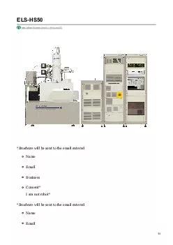
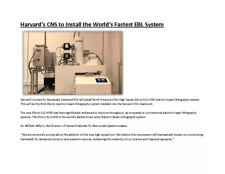
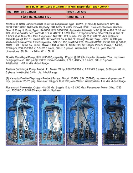
Garca Cheng Hao Lu Yonhua Manuel Muoz Yifang Chen Zhengqi Lu Yun Zhou Genhua Pan Zheng Cui and A A Pasa 1 Laboratorio de Fsica de Sistemas Pequeos y Nanotecnologa Consejo Superior de Investigaciones Cientficas CSIC Serrano 144 28006 Madrid Sp. Simonis Standard Cloth Cutting Guide for best yield use 66 wide cloth for 7 and 8 Std tables All rail cuts are 6 width No rails off the ends A u t h e n t i c A c c u r a t e A l w a y s Iwan Simonis Inc wwwsimonisclothcom 1514 St Paul Avenue Gurne It allows the measurement of magnetic fields or the detection of magnetic parts The highly sensitive and small size magnetoresistive sensors consist of a chip covered with thin film permalloy stripes These stripes form a Wheatstone bridge whose outp NOMINAL COMPOSITION Nickel 800 Silicon 35 Molybdenum 48 Iron Balance Manganese 50 TYPICAL MECHANICAL PROPERTIES ANNEALED COLD ROLLED Ultimate Tensile Strength 90000 PSI 160000 PSI Yield Strength 2 Offset 35000 PSI 150000 PSI Elongation in 2 30 1 Mo by . means of MBE method. Ashida. . lab. M1 . K. amizono Kenta. Introduction. All-optical switching devices. Excitons . and light in the high-quality system . Background . Previous results. Temperature dependence of DFWM spectrum. Michael Johnston. 4/13/2015. Abstract and Outline. Nanoscale Lithography. . is an ever growing fabrication process due to technology demands. We are continuously striving to increase the number of transistors on a chip to increase performance. The drive for smaller and faster technologies has caused the development of fabrication techniques that allow us to work at the nanoscale feature size. A few lithography techniques will be explored to show how this whole process works. The processes I will cover include Photo, Electron Beam and X-Ray lithography. These forms of lithography share a common process of preparation exposure and development while fabricating wafers.. NANO 101. Introduction to Nanotechnology. 1. 2. Lithography. Photolithography. Electron beam lithography. X-ray lithography. Focused ion beam lithography. “Photoengraving”. Transfer pattern into reactive polymer film (“resist”). EE 4611 . Dehua . liu. 4/8/2016. THE origin of Nanoscale Lithography. Major methods . of Nanoscale . Lithography. A. dvantages and disadvantages of different methods of Nanoscale . Lithography. Moore’s . Ziam Ghaznavi. CHE 384T Lithography. November 30. th. , 2017. 1. Outline/Agenda. Motivation. Ion – Solid Interactions. Overview of IBL Systems . Future Outlook. 2. Motivation. SEMATECH and the ITRS. Electron Beam Lithography System HS50 Harvard’s Center for Nanoscale Systems(CNS) will install North America’s first High Speed Elionix ELS-HS50 electron beam lithography system. This will be the third Elionix electron beam lithography system installed into the Harvard CNS cleanroom. 1989 Buss-SMS- 28LUWA 29Mfg Buss-SMS-CanzlerModel LN-0050StockNo MGAB001126Serial No1381989 Buss-SMS-Canzler GmbH Thin Film Evaporator Type 28LUWA 29 FK0234 Model and S/N LN-0050/138D-6308 Butzbach C in ASTeC. Oleg Malyshev and Reza Valizadeh. 1. The aim of TF SRF programme. SRF programme at ASTeC started six years ago from no infrastructure and it aims from beginning was to stablish know how for depositing SRF thin film in RF (. Adeetya's Kitchen & Furniture is an innovative brand that specializes in providing high-quality best Modular Kitchen Systems and Furniture to customers. https://adeetyas.com/ Best Manufacturer for Fabricated wardrobe manufacturer in Pune offered by Adeetya's Kitchen & Furniture https://adeetyas.com/fabricated-wardrobe-manufacturer-in-pune.php

Download Document

Here is the link to download the presentation.
"Magnetoresistance in Thin Permalloy Film nmthick and nm wide Nanocontacts Fabricated by"The content belongs to its owner. You may download and print it for personal use, without modification, and keep all copyright notices. By downloading, you agree to these terms.

Related Documents