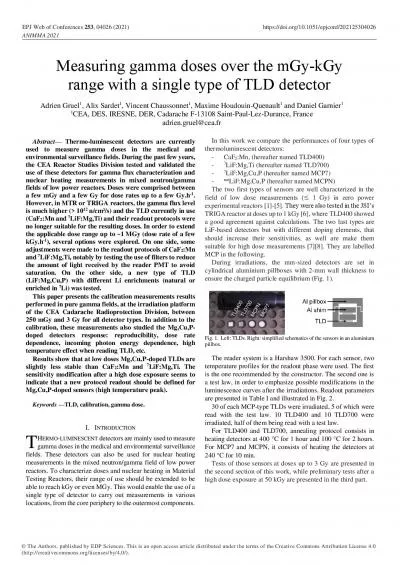
ANLFNALUCVWS Meeting Nov 28 2011 Alan Prosser CDESE Fermilab 1 Optical Communications for HLLHC Motivation Subdetectors for the HLLHC will require more ondetector communications bandwidth than is conveniently available from current optical transceivers even arrays ID: 720124
Download Presentation The PPT/PDF document "Optical Communications for HL-LHC detect..." is the property of its rightful owner. Permission is granted to download and print the materials on this web site for personal, non-commercial use only, and to display it on your personal computer provided you do not modify the materials and that you retain all copyright notices contained in the materials. By downloading content from our website, you accept the terms of this agreement.
Slide1
Optical Communications for HL-LHC detectorsANL/FNAL/UC/VWS MeetingNov. 28, 2011Alan ProsserCD/ESEFermilab
1Slide2
Optical Communications for HL-LHCMotivation Sub-detectors for the HL-LHC will require more on-detector communications bandwidth than is conveniently available from current optical transceivers (even arrays)
Increase in on-detector bandwidth requirements must be provided within
thermal and mass budgets
Past issues with VCSEL reliability indicate that a new approach NOT based upon on-detector laser sources may be favorableAn approach based on externally modulated optical communications offers advantages 1. Low on-detector power dissipation 2. High data rates 3. Improved reliability (no lasers on detector)
2Slide3
11/28/2011Proprietary3
General Link Requirements
Next generation HEP experiment requirements:
Flexible data rates (10Gbps up to 200Gbps).High reliability in a range of radiation environments.Low power consumptionSmall size (≤2-3cm
2
)
Moderate cost:
Part cost – COTS where possible (use industry standards – Ethernet, ITU, etc.)
Design and testing cost- low capital equipment (Test equipment cost becomes prohibitive with
channel speed
>10Gbps).
Installation and maintenance costs – low fiber count, small
connectors/devices
Proposed Solution: A Multi-
Gbps
(per single mode fiber) link combining:
1.
Rad
-hard, small footprint, low power optical modulator device technology
2. Wavelength Division MultiplexingSlide4
Phase Control
V
mod
3dB Optical Splitter
10-40Gbps Data Rate
InP substrate
Input Fiber:
CW laser
Output Fiber:
10-40Gbps signal
Rad
Hard Mach
Zehnder
Modulator
Key Component - Mach-
Zehnder
Modulator (MZM)
Intensity modulation achieved through phase shift of optical wave along one leg of
interferometer (phase control electrode)
Input laser operates as a continuous wave source
located off detector
(reduced detector
thermal load, no issues of
rad
-hardness for off detector laser)
Compact
rad-hard assembly needed (current COTS devices are rather large)High data rates achievable (10 Gbps – 40 Gbps in current devices) with minimal power dissipation
4Slide5
11/28/2011Vega Wave Systems Proprietary5
System Concept Proposal
Multiple CW laser diodes
λ
1
,
λ
2
…
λ
i
Receivers
Control Room
Detector/
Experiment
10Gbps per
λ
i
Mux
Demux
SM PANDA fiber
SM PANDA fiber
Wavelength Division Multiplexing (WDM) at 10Gbps/channel with external CW laser sources and modulators at the experiment.
ModulatorSlide6
11/28/2011Vega Wave Systems Proprietary6
Advantages/Features
Lower Capital Costs:
Test equipment costs lower for 10Gbps channel data rates.Minimized Cable/Infrastructure: WDM minimizes cabling from the control room.
Channel Speed Upgrade:
Modulators could upgrade speeds to 25Gbps ‘easily’ – drive electronics are the limitation.
Reliability:
Channel redundancy possible for improved reliability.
External modulators
Reduced Size:
Demux
at the detector outer layers, distribute fibers to various layers/locations on the detector.
Demux
size is less critical if located outside the detector
Integrated modulators possible.COTS Components: Lasers, receivers could be easily modified COTS parts.Modulators may need some customizationDemux/mux could be COTS.Slide7
ANL/FNAL/UC collaborative EffortAll three institutes are involved in the HL-LHC detector upgradeThey have common interest of developing a new generation of optical link based on new optical modulatorsAll three groups have the expertise and experience to pursue this type of research
Together, they will work with an industrial partner,
Vegawave
Inc. on this.Each institute will have a well defined activity during the initial phase. 7Slide8
8Collaborators, Tasks, ContributionsProof of Concept (Test System)
Collaborators:
Argonne National Laboratory
Radiation testing of commercial modulators Fermi National Accelerator Laboratory System performance testing, prototype PCB design University of Chicago Irradiation control station, radiation testing Vega Wave Systems Device fabrication, device testing
Slide9
ANL Proposed Modulator Test SetupFPGA board
PC
QSFP board
I2C Main
+ Power
QSFP board
I2C + Power
QSFP
QSFP
QSFP
InP
Receivers
LiNbO3
Electrical feedback
Radiation Exposure Region
8 SMA
USB
USB
8 Fiber
12 Fiber
MPO
4 Fiber
4Fiber
12 x fiber
fanout
12 V
2 x Differential I2C
I2C
4 fibers
4 fibers
SMA
PM Fiber
Fiber SM
Power
Power
~100 m
SMA
8 SMA
CW Lasers
Shielded from radiation
Plan to test 3 types of modulators (all @
all in-hand)
LiNbO3 (have 2) 10Gb/s,
InP
(have 1, may need to modify)
Molex/
Luxtera
(2 in hand 1 in order)Slide10
MZM x 4 (40 sq mm target)
FNAL CWDM Modulator System
40
Gbps
line rates are a challenge (design, testing, costs)
Solution – Combine MZ Modulators (4) with Coarse Wavelength Division Multiplexing (CWDM)
10
Gbps
line rates can be tested with our current equipment
Use of multiple line wavelengths and modulators reduces single point of failure issues
Wavelength implicitly encodes address of data source
+
COTS CWDM Components
10Slide11
11
Vega Wave
Systems
Fabrication
and Device Characterization
Designs and manufactures fiber optic devices and optical links for communications.
Two PhDs, 3 technicians,
5000
sf
facility with 2000sf Class 1000 clean room for semiconductor fabrication and packaging.
Semiconductor component and system test capability from DC-50GHz
Capabilities: Compound Semiconductor components and subsystems.
Laser diodes (850nm, 1300nm, 1550nm): high power and single mode.
Photodetectors
/
photovoltaics
(p-
i
-n, APD)
Silicon Optical Benches (Si v-grooves)
Fiber optic amplifiers/Fiber Lasers
TransceiversSlide12
12Extra slidesSlide13
13
Digital Signal Analyzer (Eye Patterns, Jitter)
Labview
VIs (Histogram Analysis)
Variable Optical Attenuators (Sensitivity Analysis)
FNAL Optical Test and Measurement
FPGA Signal Integrity Kit (BERT, PRBS Generation)
High Speed Optical Component
PCB DesignSlide14
1470 nm
1490 nm
1510 nm
1530 nm
SFP (
Tx
)
COTS MZM
COTS MZM
COTS MZM
COTS MZM
CWDM
Mux
CWDM
DeMux
1470 nm
1490 nm
1510 nm
1530 nm
Array Rx
Driver_Tx0
Driver_Tx1
Driver_Tx2
Driver_Tx3
SMF
SMF
SMF
SMF
SMF
SMF
SMF
SMF
SMF
SMF
SMF
SMF
SMF
FPGA
COTS MZM Driver
LVDS
LVDS
LVDS
LVDS
Rx0
Rx1
Rx2
Rx3
LVDS
LVDS
LVDS
LVDS
Rx0
Rx1
Rx2
Rx3
LVDS
LVDS
LVDS
LVDS
T
x0
T
x1
T
x2
T
x3
Driver_Tx0
Driver_Tx1
Driver_Tx2
Driver_Tx3
COTS MZM Driver
COTS MZM Driver
COTS MZM Driver
CW
CW
CW
CW
10
Gbps
10
Gbps
10
Gbps
10
Gbps
4
0
Gbps
10
Gbps
10
Gbps
10
Gbps
10
Gbps
10
Gbps
10
Gbps
10
Gbps
10
Gbps
10
Gbps
10
Gbps
10
Gbps
10
Gbps
Mach-
Zehnder
CWDM Demonstration System
Single Channel and Array Devices
Devices that need to be obtained for demo
14Slide15
15Optical Communications for Future TrackersEvolution of Versatile Link for ATLAS/CMS
Phase III R&D targeting:
1. Low Power
GigaBit Transceiver (LP-GBT) 2. Small Footprint Versatile Link Transceiver (SF-VL)The characteristics of links based on these components would be: 1. Low power laser driver for a 5 Gbps VCSEL-based transceiver for tracker applications 2. 10
Gbps
optical engine (VCSEL array) and package for calorimeter
applications
We propose to take the next step with a
Modulator Based Array