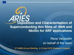
NbN and Nb3Sn for SRF applications Reza Valizadeh on behalf of the team 2 nd ARIES Annual Meeting 812 April 2019 Budapest Hungary MOTIVATION Bulk niobium Nb has been for the past three ID: 788789
Download The PPT/PDF document "Deposition and Characterisation of Super..." is the property of its rightful owner. Permission is granted to download and print the materials on this web site for personal, non-commercial use only, and to display it on your personal computer provided you do not modify the materials and that you retain all copyright notices contained in the materials. By downloading content from our website, you accept the terms of this agreement.
Slide1
Deposition and Characterisation of Superconducting thin films of NbN and Nb3Sn for SRF applications
Reza Valizadeh on behalf of the team
2
nd
ARIES Annual
Meeting
, 8-12 April 2019,
Budapest, Hungary
Slide2MOTIVATION
Bulk niobium (Nb) has been for the past three decades: the material of choice for SRF applications:It has the highest Tc (9.25K) for pure metal
It has highest
lower critical
magnetic field Hc1Easy fabricationBut it has achieved the magnetic field limitation so further improvement of cavity RF performance dictate to turn to other superconducting materials. The material can be deposited as thin film either in:Single layer (new material on Cu or Nb)Double layer ( Nb/ new matrial on Cu)Superconductor/Insulator/new material SIS
2nd ARIES Annual Meeting , 8-12 April 2019, Budapest, Hungary
2
Slide3Desired SC propertiesThe desired SC material should have the following characteristic:
A large superheating field Bsh (large Eacc)
Moderate
ξ
(not to be affected by small defects)Large Tc (RBCS ∝ e−Tc/T and small normal resistivity ρn)2nd ARIES Annual Meeting , 8-12 April 2019, Budapest, Hungary 3
Slide4SYSTEM 1
Nb3SN2nd ARIES Annual Meeting , 8-12 April 2019, Budapest, Hungary
4
Slide5Nb3Sn unit cell Structure
The Sn atoms forms a bcc lattice and each cube face is bisected by orthogonal Nb chains. In bcc Nb the shortest distance between the atoms is 0.286 nm starting from a lattice parameters of a = 0.330 nmIn Nb3SN the lattice parameters of about a = 0.529 nm for stoichiometric composition and the distance between the
Nb
atoms is 0.265 nm
The reduction of distance between the Nb chains is responsible for the high Tc in comparison to bcc Nb. Sn deficiency may cause the Nb to occupy the site and effect the long range order2nd ARIES Annual Meeting , 8-12 April 2019, Budapest, Hungary 5
Slide6Nb3Sn binary phase diagram
Intermetallic niobium–tin is based on the superconductor Nb
, which exists in a bcc
Nb
structure or a metastable Nb3Nb A15 structureWhen alloyed with Sn and in thermodynamic equilibrium, it can form either Nb1−βSnβ (about 0.18≤β≤0.25) or the line compounds Nb6Sn5 and NbSn2.
Both the line compounds at β = 0.45 and 0.67 are superconducting, with
Tc<2.8 K for Nb6Sn5
Tc<2.68 K for NbSn2
2nd ARIES Annual Meeting , 8-12 April 2019, Budapest, Hungary
6
Binary phase diagram of the
Nb
–Sn system after
Charlesworth
et al
1
970 Chapman and Hall Ltd,
Slide7Variation in lattice propertiesVariations in superconducting properties of the A15 phase are related to variations in the lattice properties through:
The lattice parameter (a) Atomic Sn content (β) The normal state resistivity just above Tc (ρn) The long range order (LRO).
2nd ARIES Annual Meeting , 8-12 April 2019, Budapest, Hungary
7
Slide8Nb3Sn deposition system and parameters
Magnetron sputtering from a RRR 300 Nb target Substrate Temperature, Deposition Rate, Deposition Thickness, Substrate Bias, Concurrent Ion Bombardment can be varied independently.
Substrates are loaded into the load lock and system fully Baked
.
Nb deposition:400 W, 470v, 0.85A4 hours depositionDc sputteringNb3Sn deposition:200 W, 489 V, 0.41 A 2 Hours deposition DC sputtering2nd ARIES Annual Meeting , 8-12 April 2019, Budapest, Hungary 8
Slide9Cu/Nb3Sn deposition (single layer)
2nd ARIES Annual Meeting , 8-12 April 2019, Budapest, Hungary 9
element
atomic %
Cu L
0.06
N L
76.76
Sn L
23.18
The lattice parameters is also been calculated to be
5.292
A
.
The
grain size calculated from the X-ray diffraction is in order of
8 to 10 nm
(Twice coherent length of
Nb3Sn which is reported to be
4.2
nm
)
Slide10Normalized DC magnetic moment
Best performance in terms of superconducting properties is achieved by the film deposited at 650 °C (A15-6) where the film deviate slightly from the Meissner state even up to a field of 300 mT.
The
film deposited at room temperature and then post annealed (A15-9) has the worst performance since M/Mi drop sharply at very low field of about 10 mT. The film deposited at moderate temperature of 450 °C performs slightly better but its performance is much reduced. This is also evident in the critical temperature of sample A15-7 where the Tc is estimated to be 14.6 K in comparison to the sample A15-6 which depicted to have Tc = 15.7.2nd ARIES Annual Meeting , 8-12 April 2019, Budapest, Hungary 10
Slide112nd ARIES Annual Meeting , 8-12 April 2019, Budapest, Hungary
11
Cu
(EP
DL)/Nb3Sn (single layer)There is some diffusion of copper at the interface
There is a clear oxide layer at the interface despite high temperature treatment prior deposition
There are area that it is Sn deficient.
Slide12Cu/Nb/NB3Sn (double layer)
2nd ARIES Annual Meeting , 8-12 April 2019, Budapest, Hungary
12
The
Nb/Nb3Sn bilayer was deposited on copper in order to compare the performance of the thin film Nb3Sn as a superconducting material suitable for SRF cavity fabrication.
Two distinct area can be observed:
Perfect area with sharp interface with correct stoichiometry for Nb3Sn layer
Copper diffusion from the interface to top surface.
Slide13Cu/Nb/NB3Sn (double layer)
2nd ARIES Annual Meeting , 8-12 April 2019, Budapest, Hungary
13
Nb
and Nb
3
Sn is completely intermixed and there is a substantial volume of copper substrate both in elemental and alloy form of copper-tin alloy is present throughout the depth of the layer and at the surface
Slide14Normalized DC magnetic moment
2nd ARIES Annual Meeting , 8-12 April 2019, Budapest, Hungary 14
In contrast with the single layer of Nb
3
Sn deposited as single layer but in exactly the same condition the onset of the drop in magnetisation start much lower field of 50 mT.The normalised magnetisation is the sum of the magnetisation of Nb layer and the Nb3Sn layerThe critical temperature of the Nb3Sn layer is found to be at 17.8 K. T
he
drop is
gradual which is can be due to presence mixed phases or area of Sn deficient or some other type of
defects.
Slide15Cu/Nb/NB3Sn (double layer)
2nd ARIES Annual Meeting , 8-12 April 2019, Budapest, Hungary
15
The interfaces both at Cu/
Nb and Nb/Nb3Sn is well defineNb layer is grown is large grain and in a perpendicular direction to the substrate surfaceNo intermixing of elements is observed Some area of Sn deficiency and are of rich Sn in Nb3Sn layer can be observed.
Slide16SIS Structure of Nb3Sn/AlN/Nb multilayer on copper
2nd ARIES Annual Meeting , 8-12 April 2019, Budapest, Hungary
16
Although the layers are well identified however there is again some degree of mixing can be observed.
Sn segregation at Cu/Nb interfaceNb3Sn into Nb layer
Copper diffusion on to the surface
Some level of Nitrogen diffusion into all the layers.
Slide17SIS Structure of Nb3Sn/AlN/Nb multilayer on Ta
2nd ARIES Annual Meeting , 8-12 April 2019, Budapest, Hungary
17
Although the layers are well identified however there is again some degree
of mixing can be observed.Sn segregation at Cu/Nb interfaceNb3Sn into
Nb layer segregated at the grain boundary
Some level of Nitrogen diffusion into all the layers.
Slide18SIS Structure of Nb3Sn/AlN/Nb
multilayer on Ta2nd ARIES Annual Meeting , 8-12 April 2019, Budapest, Hungary
18
The
layers are well identified and beside nitrogen no mixing can be observed.No Sn segregation at Ta/
Nb interface
Nb3Sn into
Nb
layer
Slide19Normalized DC magnetic moment2nd ARIES Annual Meeting , 8-12 April 2019, Budapest, Hungary
19
the deviation from the Meissner state starts at applied external field of 80
mT
which resembles to those of Nb single layer deposited on copper rather than Nb3Sn observed above which the film stayed in Meissner state up to field of 300 mT. The full cycle hysteresis loop shows a smooth curve over the full range of applied field which means that the film has stable flux pinning.
Slide20First flux entry Ben in Perpendicular Mag Filed for Nb3Sn
2nd ARIES Annual Meeting , 8-12 April 2019, Budapest, Hungary 20
The first flux entry field B
en, determined applying the 2% relative difference criterion, at 4.22 K. Comparison of all Nb
3Sn samples deposited on different substrates (Cu, Sapphire, Ta). D – indicates the damaged samples on Ta substrate.
SYSTEM 2
NbN
2nd ARIES Annual Meeting , 8-12 April 2019, Budapest, Hungary
21
Slide22NbN superconducting thin Film
2nd ARIES Annual Meeting , 8-12 April 2019, Budapest, Hungary
22
B1 compounds have a
NaCl-like structure where metallic atoms A form a face cantered cubic (fcc) lattice and non-metallic atoms B occupy all the octahedral interstices. NbN has a very complex phase diagram, which makes it very challenging to achieve the superconducting δ phase.
ɣ
-N
bN
Tc=15-17,3K
δ
-NbN
Tc=12-15K
Slide23NbN deposition parameters & subs prep
The NbN samples were synthesised in a randomized order developed through the use of a design of experiments function in Origin-Pro data analysis software
2nd ARIES Annual Meeting , 8-12 April 2019, Budapest, Hungary
23
Mechanically polished to a roughness of Sq = 35 nm
18 nm.
Ultra sonic degrease in acetone – 15
mins
Ultra sonic degrease in ethanol – 15
mins
Chemical etch in HNO
3
:H
2
O (distilled) in a 3:2 ratio – 30 seconds
Rinsed with distilled water
Blow dry with N
2
NbN film growth as function of dep parameters
2nd ARIES Annual Meeting , 8-12 April 2019, Budapest, Hungary
24
The substitution of
Ar
with Kr did not change the growth mode.
Due to parameters interdependency no significant dependency of film growth with
Ts
was observed.
Film density can be controlled
Deposition temperature
working pressure
Deposition power
Sample bias
the high tendency of patterning of the coatings due to the different crystallographic orientation of the polycrystalline Cu substrate
(a)
(b)
(c)
(d)
(e)
(f)
columnar
Dense
Slide25Ben in Perpendicular Mag Filed for N
b, NbN, Nb3Sn
2nd ARIES Annual Meeting , 8-12 April 2019, Budapest, Hungary
25
All NbN samples are considerably below the range of Ben values determined for the series of NbThe Nb3Sn samples show a wide spread of Ben values The
highest Ben’s are comparable with the highest ones of the Nb samples while the lowest Ben’s are well below the range of
Nb
samples
.
Slide26Summary
Nb3Sn can be successfully deposited from an alloy target and demonstrate good SC properties when it is deposited at high temperature (around 550-650 °C).Complex
defects can be formed in when Nb3Sn is deposited in a multilayer structure
.
NbN can be produced from an Nb metal target by reactive sputtering in N2 rich atmosphere. The optimisation of the film’s structure is possible at well selected parameter settings. If NbN can compete with Nb or Nb3Sn in terms of SC properties, it will be shown in upcoming studies. For SIS structures, the screening layer materials should be one containing nitrogen such as NbN and NbTiN, especially when the insulation layer is AlN.
2nd ARIES Annual Meeting , 8-12 April 2019, Budapest, Hungary
26
Slide27SummaryDC magnetometry
is an insufficient technique for multilayer characterisation of superconducting properties. The WP15 team should focus on development of:3rd harmonics at CEA (operational) and IEE (presently under commissioning), magnetic field penetration at STFC (presently under commissioning) and
RF measurements at CERN (operational), HZB (operational) and STFC (presently under commissioning).
2nd ARIES Annual Meeting , 8-12 April 2019, Budapest, Hungary
27
Slide28Team Members
STFCAdrain HannahGavin Stenning
Daniel
Turner
Yukari Dan (Hitachi)Karl Dawson Sepideh AliasghariStuart WildeOleg MalyshevTobias JungingerGraeme BurtVinod DannakUniversity of SiegenMichael Vogel
Stewart LeithXin Jiang
Thorsten
Staedler
2nd ARIES Annual Meeting , 8-12 April 2019, Budapest, Hungary
28
IEE
Eugen Seiler
Rastislav
Ries
INFN
Cristian
Pira
Eduardo
Chyhyrynets
Fabrisio
Stivanello
Luca
Zanotoo
Special thanks to all the team member