/
MT TUTORIAL Op Amp Output PhaseReversal a nd Input OverVoltage Protection OP AMP OUTPUT MT TUTORIAL Op Amp Output PhaseReversal a nd Input OverVoltage Protection OP AMP OUTPUT

MT TUTORIAL Op Amp Output PhaseReversal a nd Input OverVoltage Protection OP AMP OUTPUT - PDF document

sherrill-nordquist
sherrill-nordquist . @sherrill-nordquist
Follow
706 views
Uploaded On 2014-12-27

MT TUTORIAL Op Amp Output PhaseReversal a nd Input OverVoltage Protection OP AMP OUTPUT - PPT Presentation

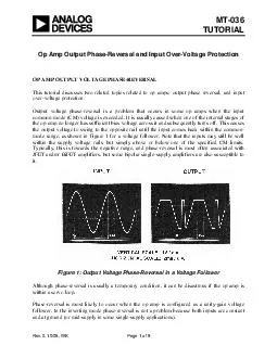
Output voltage phasereversal is a problem that occurs in some op amps when the input commonmode CM voltage is exceeded It is usua lly caused when one of th e internal stages of the op amp no longer has sufficient bias voltage acro ss it and subseque ID: 30051

Output voltage phasereversal

Share:

Link:

Embed:

Download Presentation from below link

Download Pdf The PPT/PDF document "MT TUTORIAL Op Amp Output PhaseReversal ..." is the property of its rightful owner. Permission is granted to download and print the materials on this web site for personal, non-commercial use only, and to display it on your personal computer provided you do not modify the materials and that you retain all copyright notices contained in the materials. By downloading content from our website, you accept the terms of this agreement.


Presentation Transcript

age Phase-Reversal in a Voltage Follower Although phase-reversal is usually a temporary cond MT-036 most modern op amps do not suffer from phase-reversal. If the op amp is designed to avoid phase-rein the “Key Features” table, but not n-rail" input op amps, the input CM voltaop amp should not exhibit phase-reversal as long as the input voltage does not exceed the rails. solute maximum specifications for the (quad), AD8626 (dual), and AD8627 (single) op amp family. These amplifiers have JFET inputs and an input CM voltage range of 0 V to +3 V (maximum) when operating on a single +5 V supply. The "no phase-reversal" specification means that the output will not exhibit phase-reversal in the CM Figure 2: "Key Features" and Absolute Maximum Some op amps may exhibit output voltage phase-relute maximum specification for the input voltage circuits should be added. In most cases these protection circuits will also serve to prevent output Page 2 of 9 MT-036 INPUT OVER-VOLTAGE PROTECTION AND OUTPUT PHASE-REVERSAL PROTECTION CIRCUITS The absolute maximum ratings are the voltage, current, and temperature limits beyond which an IC op amp will suffer damage. Applying over-voltages to input pins a common way to damage into two catagories: over-electrostatic discharge (ESD)ESD voltages typically are in the thousand of volts. Most of us have experienced ESD. Shuffle especially in a dry environment, and touch a metal doorknob. Sparks will fly from your fingertips. CMOS circuits are especially prone to ESD damage, but bipolar circuits can be damaged also. Most op amps have internal ESD protection diodes on the assembly phase. These diodes are small to minimize capacitance and leakage, acurrents greater than a few mA. Whenever an op amp input common mode (CM) amp can be damaged, even if the supplies are turned off. Accordingly, the absolute maximum input ratings of almost all op amps limits the grpositive and negative supply voltage, plus about 0.3 V beyond these voltages (i.e., +Vb applies even if the absolute maximum input voltage is While some exceptions to this general rule might exist it is important to note this: Most IC op The failure mechanism is not the over-voltage per e input current is limited to no more than 5 mA (a good rule of thumb), no catastrophic damage will be done. However, continually overstressing the inputs can cause a change in parameters, such as bias current and offset voltage. Even though it may not necessarily destroy the op amp, ovediodes from the input pins to miting resistors (see Figure 3). The diodes are typically Schottky diodes, used because of their lower forward voltage (typically 300 mV vs. 700 mV for silicon). caution however. Some diodes can be very current essentially adds to the op amp bias current. Some which may limit frequency response. This is especially true for high speed amps. The addition of the external current limiting resistor RLIMIT Page 3 of 9 MT-036 1N57111N5711LIMIT VIN RFB1k +VS VOUT LIMIT IN(MAX) 5mA +_ -VS CF 1N57111N5711LIMIT VIN RFB1k +VS VOUT LIMIT IN(MAX) 5mA + -VS INTERNAL ESDPROTECTION DIODES p Over-Voltage Protection Network Using Schottky Clamp Diodes with Current Limit Resistance current should be limited to 5 mA to avoid damage. This is a conservative rule of thumb, based on metal trace widths in a typical op amp input. Higher levels of current can cause hould a migration situation be present, failure may only appear after a long time due to multiple over-voltages, a very difficult failure to identify. So, even though an amplifier may appear to withstand well above 5 mA for a short time period, it is important to limit the current to 5 mA (oSome op amps, such as the , include protection diodes, but still require current limiting. If an op amp has protection diodes it will typically have a spec for maximum differential input so show up on the simplified schematic. Some op amps also have back-to-back diodes voltage protection, but to limit the maximum spec of ±700 mV for thamp CM protection circuit. With appropriate protection for a great many op amps op amp may also have internal Page 4 of 9 MT-036 diodes, so the internal units never reach their threshold. Diverting fault currents externally eliminates potential stress, protecting the op amp. freedom, some not so obvious. For example, if fault current is allowed to flow in the op amp, RLIMIT must then be chosen so that the maximum current is no more than 5 mA for the worst case V. This criterion can result in rather large LIMITand the associated increase in noise and offset voltage may not be acceptable. For instance, to protect against a V of 100 V with the 5 mA criterion, RLIMITHowever with external Schottky clamping diodes, this allows RLIMIT to be governed by the maximum allowable D1-D2 current, which can be larg care must be used LIMIT value as low as possible, to minimize offset and noise errors. LIMIT, in series with the op amp input, produces a bias-current-proportiouncorrected, this voltage appears as an increase in the circuit’s offset voltage. Thus for op amps where the bias currents are moderate and approximately equal (most bipolar types) compensation balances the dc effect, and minimizes this error. For low bias current op amps (Iwon’t be necessary. To minimize noise associated with RFIXES FOR OUTPUT PHASE–REVERSAL In many cases, the addition of an appropriate RLIMIT resistor will prevent output phase-reversal. However, many op amp manufacturer might not always give the RLIMIT resistance value se-reversal. But, the value can be determined empirically in a test set. Most often, the RLIMIT resistor value providing protection against phase-reversal will also safely limit fault current through any input CM clamping diodes. If in doubt, a nominal value of Typically, FET input op amps will need only the current limiting series resistor for protection, but bipolar input devices are best protected with this same limiting resistor, LIMIT INPUT DIFFERENTIAL PROTECTION ge common-mode conditions, which is typically associated with forward biasing ofis another equally important asp applied to certain op amps, can lead to rating characteristics. reverse junction breakdown, a second case of undesirable differential of a PN junction, the problem can be more subtle in nature. It is illustrated by the partial op amp input stage in Figure 4. Page 5 of 9 MT-036 Q2A Q1BQ2B D2D1 INPUTS Stage with D1-D2 Input Differential Over-Voltage Protection Network This circuit, applicable to a low noise op amp such as the it can be shown that voltages above about 7 V between the two inputs will cause a reverse emitter-base breakdown, even small reverse currents can cause degradation in both transistor gain and noise. After emitter-base breakdown occurs, op amp parameters such as the bias currents and noise may well be out of specification. This is usually permanent, and it can occur arly if triggered by transients. For these reasons, virtually all low-noise op amps, whether NPN n diodes such as D1-D2 across 0.6 V, protecting the transistors. on as current limiters (protection for the protection diodes) but aren’t used in all cases. For example, the doesn’t have the resistors, simply because they internally, some means of external current limiting must be provided, when and if differential over-voltage conditions do occur. Obviously, this is a tradeoff situation, so the confidence of full may provide sufficient resistanceat additional resistance isn’t internal protection. When necessary, protection diodes D1-D2, if not internal to the op amp, should be added to guarantee prevention of Q1-Q2 emitter-base breakdown. If differential transients of more than 5 V can be seen by the op amp in the application, the diodes are in order. Ordinary low capacitance diodes will suffice, such as the 1N4148 family. Add current limiting resistors as necessary, to limit Page 6 of 9 MT-036 the same degradation in performance upon break limited to 5 mA, unless the data shop amps and in-amps seem complex, yes indeed, they are! Whenever op amp (or in-amp) inputs (and outputs) go outside equipment boundaries, them. Obviously, these potentially hazardous Fortunately, most applications are contained entirely within the equipment, and usually see inputs and outputs to/from other ICs on the same power system. Therefore clamping and protection schemes typically aren’t necessary for these cases. INPUT VOLTAGES MUST NOT EXCEED ABSOLUTE MAXIMUM RATINGS(Usually Specified With Respect to Supply Voltages)Requires VIN(CM)Stay Within a Range Extending to 0.3V Beyond Rails (–V0.3V +0.3V)IC Input Stage Fault Currents Must Be Limited 5mA Unless Otherwise Specified)Avoid Reverse-Bias Breakdown in Input Stage Junctions!Differential and Common Mode Ratings Often DifferNo Two Amplifiers are Exactly the SameWatch Out for Output Phase-Reversal in JFET and SS Bipolar Op Amps!Some ICs Contain Internal Input Protection Diode Voltage Clamps, Current Limiting Resistors (or both)Absolute Maximum Ratings Must Still Be Observed Figure 5: A Summary of In-Circuit Over-Voltage Considerations ING HIGH CM VOLTAGE IN-AMP The ultimate simplicity for analog channel over-voltage protection is achieved with resistive input attenuation ahead of a precision op amp. , which is able to linearly process differential signals riding 270 V. Further, and most importaconsiderations, the on-chip resistors afford protection for either common mode or differential 500 V. All of this is achieved by virtue of a precision laser-trimmed thin-film Page 7 of 9 MT-036 15V VIN+- 500 V Input Over-Voltage Protection, One-Component Simplicity, and Fail-Safe Power-Off Operation Examination of this topology amp acts to divide down the applied CM voltage at Vsimultaneously processes the input differential mode signal Vunity. Gain errors are no more than offset voltage is no more than 0.5 or 1 mV (graThese factors combine to make the AD629 a simple, one-component choice for the protection of the input resistors safely limit fault currents. In addition, it offers those operating advantages inherent to an in-amp: high CMR (86 dB minimuthe flexibility of simple polarity changes. On the flip side of performance issues, several factors make the AD629’s output noise and drift relatively high, if compared to a lower ga These factors raise the op amp or not this is an issue relevant to an individual application will Page 8 of 9 Page 9 of 9 L OVERVOLTAGE PROTECTION ADA4091-2 is a dual micropower, single-supply, 3 MHz bandwidth amplifiers featuring nteed to operate from a +3 V to +36 V single supply as well as ±1.5 V and ±18 V dual supplies. The ADA4091-2 has overvoltage protection making the device ideal for rApplications for these amplifiers include portable telecommunications equipment, power supply nd interface for transduREFERENCES: Hank Zumbahlen, Basic Linear Design, Analog Devices, 2006, ISBN: 0-915550-28-1. Also available as Linear Circuit Design Handbook , Elsevier-Newnes, 2008, ISBN-10: 0750687037, ISBN-13: 978-0750687034. Chapters 1 and 11. Walter G. Jung, Op Amp Applications Analog Devices, 2002, ISBN 0-916550-26-5, Also available as Amp Applications Handbook , Elsevier/Newnes, 2005, ISBN 0-7506-7844-5. Chapter 7. Copyright 2009, Analog Devices, Inc. All rights reserved. Analog Devices assumes no responsibility for customer product design or the use or application of customers’ products or for any infringements of patents or rights of others which may result from Analog Devices assistance. All trademarks and logos are property of their respective holders. Information furnished by Analog Devices applications and development tools engineers is believed to be accurate and reliable, however no responsibility is assumed by Analog Devices regarding technical accuracy and topicality of the content provided in Analog Devices Tutorials.