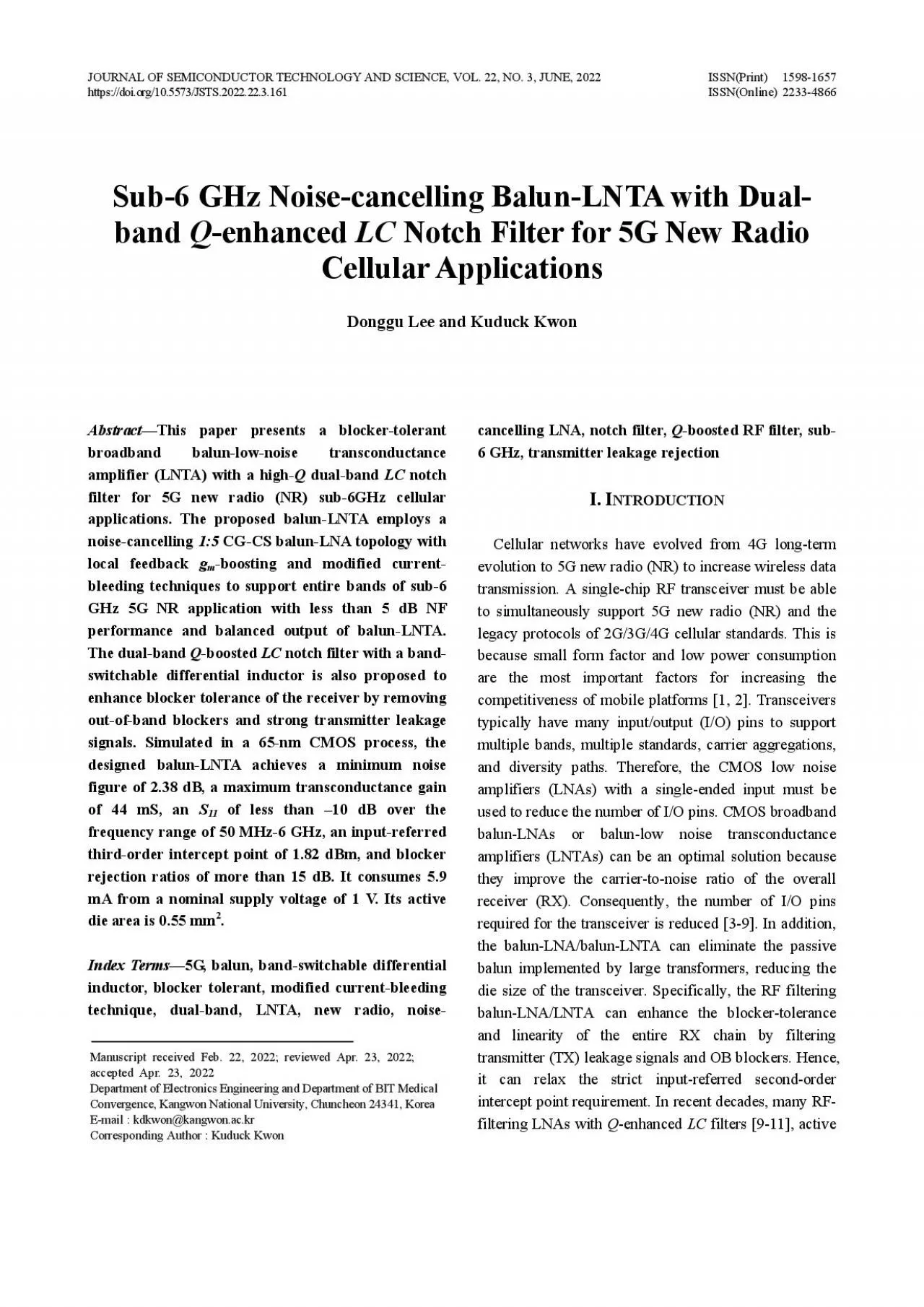
PDF-JOURNAL OF SEMICONDUCTOR TECHNOLOGY AND SCIENCE VOL 22 NO 3 JUNE

Author : tabitha | Published Date : 2022-08-16

Manuscript received Feb 22 2022 reviewed Apr 23 2022 accepted Apr 23 2022 Department of Electronics Engineering and Department of BIT Medical Convergence Kangwon

Presentation Embed Code

Download Presentation

Download Presentation The PPT/PDF document "JOURNAL OF SEMICONDUCTOR TECHNOLOGY AND ..." is the property of its rightful owner. Permission is granted to download and print the materials on this website for personal, non-commercial use only, and to display it on your personal computer provided you do not modify the materials and that you retain all copyright notices contained in the materials. By downloading content from our website, you accept the terms of this agreement.

JOURNAL OF SEMICONDUCTOR TECHNOLOGY AND SCIENCE VOL 22 NO 3 JUNE: Transcript


Manuscript received Feb 22 2022 reviewed Apr 23 2022 accepted Apr 23 2022 Department of Electronics Engineering and Department of BIT Medical Convergence Kangwon National University Chunche. 54 Cont act resistance to a thin semiconductor layer The contact between a metal contact and a thin conducting layer of semiconductor can be described with the resistive network shown in Figure 35 which is obtain 20062009 All rights reserved Pressure Integrated Silicon Pressure Sensor OnChip Signal Conditioned Temperature Compensated and Calibrated The MPX4250 series piezoresistive transducer is a stateoftheart monolithic silicon pressure sensor de signed f Lorelei Lewandowski. 4/20/2015. There are 7 II-VI semiconductor materials. Because of their direct, wide band gap energy, they are becoming increasingly useful in optical applications. While some of them have been around for many years, research is still needed to determine the full potential of others. The “latest and greatest” technology in the near future will most likely owe much of its success to these materials.. itrs. ). Kelsey Miller. 4/29/2016. Abstract: The United States semiconductor . i. ndustry is supported by the Semiconductor . Industry Association which lobbies for policies favorable for industry and helps create goals along with other top semiconductor producing regions through the International Technology Roadmap for Semiconductors. . Lorelei Lewandowski. 4/20/2015. There are 7 II-VI semiconductor materials. Because of their direct, wide band gap energy, they are becoming increasingly useful in optical applications. While some of them have been around for many years, research is still needed to determine the full potential of others. The “latest and greatest” technology in the near future will most likely owe much of its success to these materials.. Bami Bastani is the Senior Vice President for the CMOS, RF and ASIC Business Units at GLOBALFOUNDRIES. Dr. Bastani has more than 35 years of experience in high - tech industry, spanning from semico Title Comments Jiangsu Yangdian Science and Technology Co., Ltd. engages in R&D , production and sale of power transformer, iron core, amor phous and nanocrystalline magnetic electronic components NSF 21-112Dear Colleague Letter CISE RFI on Semiconductor Research andEducationAugust 5 2021Dear Colleaguesimpacts are increasingly important to the Nations long-term competitiveness and securityThe c L14. Lecture . 14: . Radiation detectors III. Germanium detectors. Interactions in surroundings. Graded shielding. Linear Attenuation Coefficients. Build-up factor. Spectrum Analysis. PHYS389 : Semiconductor Applications L14. : X-ray spine showedand second branchial arches that isinvolvement of the vertebral, renal and ocular Fig. 1 : 688Bombay Hospital Journal, Vol. 50, No. 4, 2008 Recently Mental deficiency isDepartment Asma. . Alwaei. Review of Semiconductor Physics. a) Energy level diagrams showing the excitation of an electron from the valence band to the conduction band.. The resultant free electron can freely move under the application of electric field.. A Brief look into the dangers of the manufacturing process, behind today’s technology. Nathan Insixiengmay. EE 4611. Outline. The Widespread Reach. The Problem. The Effect on The Community. The Solution. 1. Lecture . 13: . Radiation detectors II. Germanium detectors. Planar. Coaxial. Energy resolution. Efficiency. PHYS389 - Semiconductor Applications L13. 2. Interaction of gamma-rays with matter. Gamma radiation is a very penetrating form of radiation that does not directly ionise the material through with it travels.. Semiconductor detectors have a . high density. . . ● large energy loss in a short distance. . ● diffusion effect is smaller than in gas detectors resulting in achievable position resolution of less then 10 .

Download Document

Here is the link to download the presentation.
"JOURNAL OF SEMICONDUCTOR TECHNOLOGY AND SCIENCE VOL 22 NO 3 JUNE"The content belongs to its owner. You may download and print it for personal use, without modification, and keep all copyright notices. By downloading, you agree to these terms.

Related Documents