/
Ion Implantation Advantages  Precise control of doping levels  Measure Ion Implantation Advantages  Precise control of doping levels  Measure

Ion Implantation Advantages Precise control of doping levels Measure - PDF document

tatiana-dople
tatiana-dople . @tatiana-dople
Follow
397 views
Uploaded On 2015-11-03

Ion Implantation Advantages Precise control of doping levels Measure - PPT Presentation

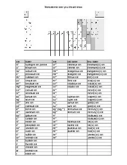
Ion Implant useful Formulas Energy Ei in each ion is in electron Volts ZeVmvEi221 Where V accelerating voltage Volts v velocity of the ion m mass of the ion Z e charg ID: 181427

Ion Implant useful Formulas

Share:

Link:

Embed:

Download Presentation from below link

Download Pdf The PPT/PDF document "Ion Implantation Advantages Precise con..." is the property of its rightful owner. Permission is granted to download and print the materials on this web site for personal, non-commercial use only, and to display it on your personal computer provided you do not modify the materials and that you retain all copyright notices contained in the materials. By downloading content from our website, you accept the terms of this agreement.


Presentation Transcript

Ion Implantation Advantages Precise control of doping levels Measure dopants dose in atom/cm2 Much less dopant spreading (sideways & down) Needed for small structures Implanters expensive $1 - $2 million To get depth may need high voltage/high current double or triple ionized Heavy radiation damage to crystal Dopant need to be activated (go interstitially) Implant creates high temperature in resist Resist very hard to strip Ion Implant useful Formulas Energy Ei in each ion is (in electron Volts) ZeVmvEi221 Where V = accelerating voltage (Volts) v = velocity of the ion m = mass of the ion Z = e charges on the ion (number of charges) e = electron charge = 1.60x10 C Thus 1 eV = 1.60x10 Implant values are given as beam current in Amps current is same if either electrons or ions Total implant dose Q is ZeAItQ Where I = beam current (Amps) t = implant time to scan area (sec) A = area (sq cm) Energy from ions are deposited throughout stopping range Dopant Range with Implanter Ions follow a Gaussian atomic stopping range p2p2ppR2QNorR2RxexpR2QxN Peak range = Rp Straggle of range width of Gaussian (Rp Both function of ion type, energy, and target (cross section for stopping in material) Implanter Projected Range Rp Varies with accelerating voltage & dopant Ions & targets have different interaction cross sections Calculated using complex stopping calculations Implanter Straggle Rp Varies with accelerating voltage & ion Normal straggle Rp is into depth Transverse straggle R is sideways under mask edge Range and Straggle tables Implant Rp , Rp, for common ions and energies in Silicon Implant Rp, Rp, for 100 KeV Boron in different materials Spreading of Implant Dopant from Opening Scattering of ions causes dopant to spread to side Note peak begins to die off before edge of mask Here assuming no implant through mask (not always true) Implant Penetration Through Masks Implant has dopant profile in mask but for mask material Note resist much less stopping power than oxide May result in penetration below mask Get tail of Gaussian Calculate total dopant using Buried Junctions with Implant Peak implant dopant is not at surface Thus can get n p n junctions with 1 implant Junction where implant falls below background Nb Implant Variation with Crystal Angle ᄀ Called Channeling of dopant Solved by putting off axis implant Dopant Depth with Implanter Voltage Higher implant voltages: greater depth Note deviation from true Gaussian: Light ions (eg Boron) backscatter from Si More dopant on surface side than with Gaussian Heavy ions (eg. Arsenic) forward scattered (more As deeper) Calculation of Implant Effect Use Monte Carlo method to show ion spread Trace path of single ion as moves through crystal Random process included Launch a few million ions and measure final distribution eg program: Pearson Type IV distributions Crystal Damage of Implant Low does: only local damage – little effect on crystal Medium does: large damage at ion point and in path High dose: amorphousize layer Increasing implants, increasing damage Damage areas reduce carrier velocity, create traps Gives poor semiconductor device characteristics Implant Crystal Damage Implant badly damages crystal Can turn single crystal Si into amorphous film Reduced by heating target - anneals out damage Also remove damage by raising crystal temperature after implant Ion Implant and Dopant Locations Recall dopant atoms must be substitutional: for activation Ion implant tends to create Interstitial dopant: pushes out Si Interstitial mplant ions do not contribute carriers True Interstitial dopant atoms: not activated Annealing Damage & Activating Dopants Need to heat surface to remove damage As implant level increases activation ratio decreases Heat moves dopant atoms into substitution point By 1014 less than 10% activated at implant Hence heating needed to activate Must reach a critical temperature ~800-900o Implant Activation Defect Healing Heating to remove crystal electrical damage )Primary Damage Dopant activation second requirement Problem: High temperature cause dopant to diffuse Activation changes dopant profiles! Rapid Thermal Annealing Furnace activation moves dopant around: changes profile Use light to heat only dopant surface Reach high local temperature: rapid healing/activation Rapidly cools when light off Little chance for dopant diffusion Rapid Thermal Annealing Systems Lasers expensive, heat small area Use light box of Halogen Heat Lamps Raises temperature of whole surface in seconds Can actually melt wafer surface Water cool back of target As only heat surface (not whole wafer) cools quickly Dopant Movement in Later Processes All later thermal processes change dopant positions Thermal processes cause diffusion Hence must adjust profile to take into account following processes Called process integration Oxidation Dopant Segregation Oxidation causes N dopant to pile up at surface Oxidation causes P dopant depletion (into oxide) Silicon Etching (Ruska Ch. 6) Poly Crystalline Silicon widely used as a conductor Called Poly Si: Modest resistance conductor Usually highly doped silicon Gate conductor in self aligned process Gate creates the position of the source/drain Poly Silicon etches similar to single crystal Si Changes depend on crystal size and doping Nitric oxidizes the silicon Typical Isotropic Silicon Etches Typically dilute with Acetic acid CH3 Reduces the etch rate Diluted HF/Nitric/Acetic Etch rates depend on dilution Common PolySilicon Etches Similar to single crystal Must control etch rate Anisotropic Etching of Silicon Etching that proceeds along crystalline planes ᄐ typically က () Used extensively in micromachining & power transistors က ᄀ Typical Anisotropic Etchants of Silicon EDP (Ethylenediamine Pyrocatecol & water) most common Advantages: attacks silicon, not oxide or aluminum Disadvantage: poisonous Potassium Hydroxide (KOH) Advantages: good crystal plane selectivity silicon Advantages: attacks aluminum Aluminum Multilayer Structures Aluminum most common conductor in CMOS Conductive and easy to deposit Easy to etch Problem is to make multilevel structures Must make contact between Al layers Aluminum grows a protective insulating oxide Ohmic Contacts Aluminum oxide can create diode like contacts Want a pure Ohmic contact (linear resistance) Get this by sinter in dry nitrogen at end Typical 450oC for 30 minutes Removes the oxide, creates ohmic contact Aluminum Alloys Pure aluminum has reliability problems Sinter & high temperature creates difficulties Add Copper and Silicon Makes it much harder to etch Aluminum Spike Through When Aluminum heated penetrates silicon Si moves in Al, Al into Si Get spikes which can short junctions Suppressed by adding 1-2% Si to Al Phase diagram Silicon 1.5% Aluminum Eutectic Lowest melting point alloy Preventing Spike Through Adding Si to Al prevents spikes Also put down Barrier metal layers Tungstan, Molybdenum most common Refractory metals Aluminum and Hillocks When Al heated grows Hillocks Spikes up to 1 micron high! Can punch through intermetal glass layers Add copper to suppress Also for electromigration: tendency of metal to move when current applied Problem is Si/copper makes etching difficult Aluminum Etching Oxidation: removal of electrons or ions from material M+ + e - Reduction: addition of electrons to reactant Redox reaction: both oxidation and reduction Aluminum etches are redox reactions 6H+ + Al 3 H2 + Al3+ Must remove aluminum oxide for reaction Typical Aluminum Etchants Most are Phosphoric Acid based (H3 Acetic for dilution Note: without oxide Al would etch in water Creating a Sloped Sidewall for Al Want sloped sidewall for step coverage Thus over etch aluminum Allow resist to lose adhesion Sand Removal in AlSi or AlSiCu Metal etch leaves Al rich Si sand Copper makes reaction worse must remove with a "sand remover" wet etch 29% H2O, 70% HF, 1% HNO3 Lift Off Techniques Put defined resist below metal deposition Al goes through holes Then dissolve resist Extra Al floats away Problem is the "Sky is Falling Syndrome" material left behind Assume film thickness varies by Ion Implantation Most modern devices doped using ion implanters Ionize gas sources (single +, 2+ or 3+ ionization) Accelerate dopant ions to very high voltages (10-600 KeV) Use analyzer to selection charge/mass ratio (ie ionization) Bend beam to remove neutral Raster scan target: implant all areas at specific doping Just integrate charge to get total dopant level for wafer