/
Ultrahigh-resolution spin-resolved ARPES of novel low-dimen Ultrahigh-resolution spin-resolved ARPES of novel low-dimen

Ultrahigh-resolution spin-resolved ARPES of novel low-dimen - PowerPoint Presentation

tawny-fly
tawny-fly . @tawny-fly
Follow
403 views
Uploaded On 2016-12-11

Ultrahigh-resolution spin-resolved ARPES of novel low-dimen - PPT Presentation

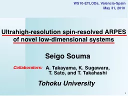
Seigo Souma Tohoku University May 31 2010 A Takayama K Sugawara T Sato and T Takahashi Collaborators 1 WS10ETLODs ValenciaSpain Anomalous electron spin phenomena Spin dependence of electronic structure ID: 500306

surface spin energy 111 spin surface 111 energy resolved arpes resolution band mott mev structure rashba rsi high effect

Share:

Link:

Embed:

Download Presentation from below link

Download Presentation The PPT/PDF document "Ultrahigh-resolution spin-resolved ARPES..." is the property of its rightful owner. Permission is granted to download and print the materials on this web site for personal, non-commercial use only, and to display it on your personal computer provided you do not modify the materials and that you retain all copyright notices contained in the materials. By downloading content from our website, you accept the terms of this agreement.


Presentation Transcript

Slide1

Ultrahigh-resolution spin-resolved ARPES of novel low-dimensional systems

Seigo

Souma

Tohoku

University

May 31, 2010

A. Takayama, K. Sugawara, T. Sato, and T. Takahashi

Collaborators:

1

WS10-ETLODs, Valencia-SpainSlide2

Anomalous electron spin phenomena

Spin dependence of electronic structure

Rashba

effect

Spintronics

Topological insulator

Bi

2

Te

3

Y.L.Chen

et al

.,

Science

325

(2009) 178.

Spin-orbit interaction

High-resolution spin-resolved ARPES

Electronic-field induced spin-current

Rashba

term

Spin switch via S.O. interaction

Edge state (surface state)

Time reversal invariant

E

(

k

,

)

=

E

(-

k

,

)

2Slide3

Spin-splitting of surface

Rashba

effect

V

= (

0, 0, Ez)Surface Rashba

effectSpin-orbit interaction

surface potential

Effective magnetic field

spin-resolved ARPES

Time reversal symmetry

E

(

k

,

)

=

E

(-

k

,

)

3

Space inversion symmetry

E

(

k

,

)

=

E

(-k

,↑) Slide4

Angle-resolved PES (ARPES)

e

-

freedom

Energy

Momentum

4Slide5

Detection of electron spin is difficult !!

Efficiency of instrument goes down by

3-4 order

Energy Resolution 100

meV

Spin-resolved ARPES

e

-

freedom

Energy

Momentum

Spin

5

Mott scattering

Mini Mott Detector

25

keVSlide6

c

6

Recent spin-resolved ARPES studies

VLEED

Mott detector

Mott detector

(retarding-type)

(high-energy type)

D

E = 30

meV

D

E = 70

meV

D

E = 70

meV

(Fe(001)p(1x1)-O)

Sb(111)

Bi

1-x

Sb

x

(x=0.13)

[9] A.

Nishide

et al., PRB

81

(2010) 041309(R).

[8] T. Okuda et al., RSI

79

(2008) 123117.

[1] K.

Iori

et al., RSI

77

(2006) 013101.

[2] S.

Qiao

et al., RSI

68

(1997) 4390.

[3] T.

Kadono

et al., APL

93

(2008) 252107.

[1,2]

[3]

Au(111)

Mott scattering

E

K

= 25

keV

Mott scattering

E

K

= 60

keV

Electron diffraction

E

K

= 6

eV

[6] M.

Hoesch

et al., PRB

69

(2004) 241401(R).

[5] M.

Hoesch

et al., JESRP

124

(2002) 263.

[7] R.

Bertacco

et al., RSI

73

(2002) 3867.

[4] V. N.

Petrov

et al., RSI

68

(1997) 4385.

[4,5]

[6]

[9]

[7,8]Slide7

High-resolution spin-resolved photoemission spectrometer

7Slide8

A

B

C

D

Spin-resolved ARPES system

8

P

z

P

y

(A,B)

(C,D)

Spin polarization

x

y

z

Spin-integrate

ARPES

Energy

Angle

Spin-resolved

ARPES

spin up

spin

downSlide9

Energy resolution at MCP

Au

metal

T = 3.5 K

Nb

superconductor

simulation

BCS function

Tc = 9.2 KGap size

D

= 1.5 meV

Broadening

G

= 200

m

eV

900

m

eV

T = 3.5 K

simulation

FD function

Energy resolution at MCP

Xe I

8.437 eV

Xe I

8.437 eV

9Slide10

High-resolution spin-resolved photoemission spectrometer

10

S. Souma et al., RSI

78

(2007) 123104.

Xe

I photons8-11

eVIntensity

2 x

10

13

photons/sec

Operation pass energy

Ep

= 1,2,5

eV

Energy resolution @ Mott

= 8-40

meV

Ep

: pass energy

Energy resolution @ Mott

~ 0.008Ep

eVSlide11

Side view

High-resolution spin-resolved photoemission spectrometer

11Slide12

Discharge problem

Au4f

ch1

ch2

12

ch2

ch1Slide13

Solving for discharge of Mott detector

Channeltron

Scattering chamber

Feed through

Safety cover

To HV supply

Au target

Focus cup

Channeltron

Scattering chamber

Focus cup

25000 V

2200 V

1300 V

Spark

Solutions

1.

Re-polishing of high voltage electrodes

3

. Washing all parts

4

. Baking

5

. Conditioning of electrode’s surface by applying HV

Field emission

BG noise depends on voltage difference between the electrodes

Roughness of surface

2

. Coating of electrodes with

TiC

13

100,000 cps

@18kV

0.1 cps

@25kV

Noise at

channeltronSlide14

Test measurement with gold sample

ch

A

ch

Bch C

ch D

AuHe Ia

T=300K

Ep 10eV

ch A

ch B

ch C

ch D

Au

T=10K

Ep 1eV

Xe

I

8.437

eV

14

Energy resolution @ Mott

= 8

meVSlide15

Peculiar surface states of group-V semimetals

Surface

Rashba

effect

with S.O.

without S.O.

Yu. M.

Koroteev

et al

.

,

PRL

93

(2004) 046403.

semimetal

Surface

peculiar metal

Bi,

Sb

bulk

15

Crystal structure of BiSlide16

16

Previous spin-resolved ARPES studies

Bi(111) film

H.

Hirahara

et al., PRB 76 (2007) 153305.Slide17

In-situ preparation of Bi thin film on Si(111)

Si

(111) 7×7

Bi

(111) 1×1

LEED

substrate

Flash annealing

Bi thin film (80ML)

epitaxially

grown on Si(111) surface

17Slide18

ARPES spectra of Bi(111) surface

s

urface

BZ

bulk

BZ

(111)Xe I (8.436

eV)T = 30 K

Experiment

18Slide19

Band structure of Bi(111) surface

19Slide20

Spin-integrate band structure of Bi(111) surface

20Slide21

Binding Energy (

eV

)

0.10

0.150.20

0.05E

FWave vector kx (Å-1)

0.0-0.2

-0.8

-0.6

-0.4

0.2

Electronic structure near E

F

of Bi(111) surface

Wa

ve vector

k

x

-1

)

0.0

-0.2

-0.8

-0.6

-0.4

0.2

Wa

ve vector

k

y

-1

)

0.0

0.1

0.05

-0.05

hole pocket

electron pocket

hole pocket

electron pocket

21Slide22

Spin-resolved ARPES of Bi(111) surface

Binding Energy (

eV

)

0.1

0.2

EF-0.2-0.4

00.2

B

G

Wave Vector

k

x

-1

)

y

z

up spin

down spin

z

direction

Intensity (

arb

. units)

Binding Energy (

eV

)

0.1

0.2

E

F

up spin

down spin

Intensity (

arb

. units)

y

directionSlide23

Binding Energy (

eV

)

0.1

0.2

EF

Wave Vector kx (Å-1)-0.2

-0.40

0.2

Problem in Bi(111) surface state

Time reversal symmetry

E

(

k

,

)

=

E

(-

k

,

)

Degeneracy of surface band at

G

(

k

=0) point

Sb

(111)

Bi

(111)

Bi(111): surface band is

unclear at

G

due to

bulk band projection

ARPES

on Sb(111)

same crystal structure

no bulk projection at

G

near E

F

23Slide24

Band structure near E

F

of Sb(111) surface

24

K. Sugawara et al.,

 PRL 96 (2006) 046411.Slide25

Band structure near E

F

of Sb(111) surface

25

K. Sugawara

et al

., PRL 96 (2006) 046411.Slide26

Surface band of Sb(111) at

G

point

2

nd derivative

26

K. Sugawara

et al

.

,


PRL

96

(2006) 046411.Slide27

Spin-resolved ARPES spectra of Sb(111)

spin up

spin

down

Bulk band

Surface band

27

K. Sugawara

et al

.

,


PRL

96

(2006) 046411.Slide28

SUMMARY

Spin-resolved ultrahigh-resolution ARPES study of

Rashba

effect on semi-metal surface

Energy resolution

D

E= 8 meV Observation of Spin-splitting of surface band on Bi and

Sb (111)Time reversal symmetry holds at

G

Surface

Rashba

effect on group-V semimetal surface