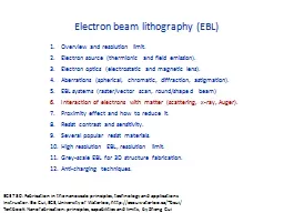
/
High brightness electron beam from a multi-walled carbon High brightness electron beam from a multi-walled carbon

High brightness electron beam from a multi-walled carbon - PDF document

trish-goza
trish-goza . @trish-goza
Follow
396 views
Uploaded On 2016-12-21

High brightness electron beam from a multi-walled carbon - PPT Presentation

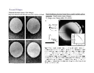
nanotube Small source many fringesN Jonge et al Nature 420 393 2002 Thermal electron source Few fringeshttpemoutreachucsdeduwebcourseSecIDSecIDhtml Fresnel Fringes J Elec M ID: 504342

nanotube : Small source many

Share:

Link:

Embed:

Download Presentation from below link

Download Pdf The PPT/PDF document "High brightness electron beam from a mul..." is the property of its rightful owner. Permission is granted to download and print the materials on this web site for personal, non-commercial use only, and to display it on your personal computer provided you do not modify the materials and that you retain all copyright notices contained in the materials. By downloading content from our website, you accept the terms of this agreement.


Presentation Transcript

High brightness electron beam from a multi-walled carbon nanotube : Small source many fringes:N. Jonge, et al. Nature 420, 393 (2002) Thermal electron source. Few fringeshttp://em-outreach.ucsd.edu/web-course/Sec-I.D/Sec-I.D.html Fresnel Fringes J. Elec. Microscopy, 22 (1973) 141 Maxima when constructive interference occurs betweenstraight beam and scattering beam at edge of sample when defocused. sample D = Defocus a x D = Defocus screen Fresnel Fringes (W&C 27.7, Fig. 5.13, 9.20; C. Hall, “Intro. to E.M.”)•Fringes at sample edges or boundaries seen only in out of focus images •Fresnel zone theory gives the position of fringe maxima:•Would continue indefinitely laterally if electron source was a point = 0; ... 3 2, 1,n )8/5(2 r source d • If d finite: The distance x at which sample xL I screen q Dd xm • If d finite: The distance x at which the fringes disappear will be such that the path difference is on the order of a wavelength. Hence: x rLddrLxddrLxll l )()(++= D So, the smaller the source the larger and hence the number of fringes Phase Contrast W&C Chap. 27Electron optics and sample introduce phase differences between transmitted and scattered beams which then are recombined by objective lens, producing lateral amplitude fluctuations. Lattice Fringes (section 27.2)•Fringes that occur with a period comparable to the atomic lattice 1 nm.•Obtained by allowing more than one beam to interfere by using a larger objective aperture (or no aperture at all)•Assuming a thin sample where we can ignore dynamical scattering effects: sin(cos((][2 andsin whereandconstant a assumingwheretsABABABBetstsBeDI y ppdppxpjjjj y dpdpdppdpp--+=+·++=+++=+=-===»+=++=+=+·-+·+····    sin(tsABs = 0 only a sinusoidal function parallel to and of spacing 1/g’= hkls ¹¹0 then a small shift depending on thickness and |s|No direct relationship to the position of actual atoms in the sample. Need computer simulation to interpret a lattice image and then must have avery thin sample (no absorption, no multiple scattering) –Weak phase object . Good example of problem see Si 110�.08;饆怀 lattice image: Fig. 27.3 W&C. SF InGaAs (14% In)/ GaAs (001) 110�.08;饆怀 TEM cross-section(JEOL 4000,0.18 point to point resolution)SF has a small shift along the line intercepting the two regions. 112&#x-2.6;昂 111&#x-2.6;昂 Interfacesomewherehere InGaAsGaAs Lab #1 polycrystalline Aluminum , 200 keV •Example from a Tecnai image taken by Ryan and Shawn Penson (2007 students).•Finer fringes are lattice fringes•Larger ones are moiréfringes from overlapping grains•No fringes visible does not necessarily mean amorphous since grains probably misaligned Fringe spacings: 0.25 ±0.01nm(Al 111= 3 = 0.234 nm)Angles between the two rows 70.5also correct for {111} planes. ZnSe nanowire:zincblende –wurtzite stacking faults. Fringe spacings: 0.35 ±0.02nm MoiréFringes Two overlapping fringe images, translational, rotational or a combination:Translational DDtm= Rotational DDrm = 2gsin(bb/2)sin[tsABts]))x(ggAB2/sinsin g1g2 Dgrg1 b 10 nm g2 GaSb on GaAs Fine fringes perpendicular to g = 004translational Moirspacing 2.1 nmFe/GaAs (001)translational Moir Moiré Fringe and Dislocation Spacing Prediction GaSb/GaAs GaAs: = 5.65 AGaSb: a= 6.10 AMismatch = f = a/a= 0.08 = 8%If the interfacial dislocations are pure edge type: Spacing of dislocations to relieve all mismatch strain along 110�.09;គ : 110  Black lines are dislocations with average spacing 5 nm. Moiréfringe spacing along the 100�.08;饆怀 direction is 1.8 nm or tm= 1/1.8 = 0.55 nm-1Predicted Moiré spacing tm= gGaAs–gGaSb= (4/0.565)-(4/0.61) = 0.52 nm-1 5008.06.5 High Resolution Imaging 1.Our sample consists of a certain density of material (r). The diffracted wave amplitude is mathematically the Fourier transform of (r)This is just the structure factor again. ))+¥ (r)Objective lens Diffraction patternIf (r)has short periodicities (eg. atomic planes) then F contains large reciprocal lattice D ))iH  D-r Image: [ ] ))iH  D--r then F contains large reciprocal lattice vectors: D k eg. r = 0.2 nm, k = 1/r = 2sin= 5 nm-12.The electron microscope objective lens adds a phase distortion function to the sample scattering factor called the:contrast transfer function H(k ) worse for higher k (larger scattering angles)Adds a phase factor to F: Contrast Transfer Function H(k ) (W&C pg. 463)Each point on the sample will be imaged as a blurred disk with a radius as a function of spherical aberrations ()and defocus of the objective lens: if f = 0 there still is the objective lens spherical aberationWe average this over all scattering angles to get the average blurred disk:Phase angle 4 2 2 ) ( 2)(42)()()(424203Cf D nm l p q l p c qqqqdqqqqdq         + D = = +D==+D= Surfaces of Where A(u) is an amplitude function related to the objective aperture.Both are sample independent, depends on your microscope objective lens and your choice of . sinsin 4 2 ) ( (radians) (nm u D 1- l q l c =D+D=+D=º»=       + = = Sample and lens Surfaces of constant phasePhase varies laterally 0 2 4 6 ReciprocalLatticeVector(u(nm-1)) -2 -1 0 1 2 TransferFunction(2sin =1mmf=-58nm 0 2 4 6 ReciprocalLatticeVector(u(nm-1)) -2 -1 0 1 2 TransferFunction(2sin =2.0mmf=-58nmPlots of 2sin as a function of and f . 0 2 4 6 ReciprocalLatticeVector(u(nm-1)) -2 -1 0 1 2 TransferFunction(2sin = 1.0 mmf = -58 nm = 1.2 mmf = -58 nm = 2.0 mmf = -58 nm = 1.2 mmf = 0 0 2 4 6 ReciprocalLatticeVector(u(nm-1)) -2 -1 0 1 2 TransferFunction(2sin 0 2 4 6 ReciprocalLatticeVector(u(nm-1)) -2 -1 0 1 2 TransferFunction(2sin = 1.2 mmf = -63 nm = 1.2 mmf = -100 nmTecnai 20 at 200 keV 0 2 4 6 ReciprocalLatticeVector(u(nm-1)) -2 -1 0 1 2 TransferFunction(2sin 2 / 1 4322233432 4 du   The ideal shape of sin as a function of is one that is flat over the largest reciprocal frequenciesOptimal condition for the best resolution?Phase angle (combining focus and aberration constant)To find the zero slope relationship between and , , and (1)(2) Best curve is when is near -120°(-2/3) 4/34/14/34/1 2 / 1 66.05.1 4 SchSchSchSch    Combining (1) and (2) gives best focus value called:Scherzer defocus Cross-over u atSch when = 0Scherzer resolution Tecnai 20 : 1.2 mm; = 0.0025 nm: Sch= -63 nm; Sch= 4.0 nm-1; Sch= 0.25 nmFor larger (smaller real space distances) phase angle rapidly oscillates and will not translate sample information reliably. Minimum contrast is what we have called focus. (28.9)This occurs when: sin ~0.3or MC= -0.44 (C1/2= -25 m (Tecnai at 200 keV)On the TEM the in situ Fourier analysis of the image that you can use to adjust astigmatism is essentially this contrast transfer function.Bright rings are when 2sin = 2and (u) = n/2 with n oddand dark rings when 2sin = 0 and (u) = n/2 withevenWe can measure the microscope using these fringe spacings. (Fig. 30.6) 2 0 2 4 6 8 ReciprocalLatticeVector(u(nm-1)) -2 -1 0 1 2 TransferFunction(2sin