/
Lecture:   Semiconductors and recombination Lecture:   Semiconductors and recombination

Lecture: Semiconductors and recombination - PowerPoint Presentation

valerie
valerie . @valerie
Follow
342 views
Uploaded On 2022-02-10

Lecture: Semiconductors and recombination - PPT Presentation

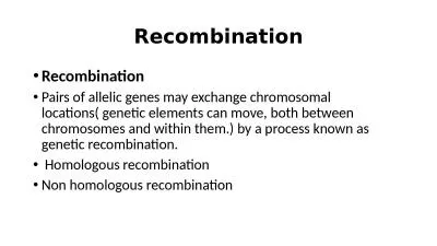
Prof Ken Durose University of Liverpool Outline semiconductors and recombination 1 Band gap representations 2 Types of semiconductors Adamantine semiconductors Hume Rothery 8N coordination rule ID: 908153

state recombination solid gap recombination state gap solid semiconductor semiconductors site iii cdte devices electrons band oxidation electronic electron

Share:

Link:

Embed:

Download Presentation from below link

Download Presentation The PPT/PDF document "Lecture: Semiconductors and recombinat..." is the property of its rightful owner. Permission is granted to download and print the materials on this web site for personal, non-commercial use only, and to display it on your personal computer provided you do not modify the materials and that you retain all copyright notices contained in the materials. By downloading content from our website, you accept the terms of this agreement.


Presentation Transcript

Slide1

Lecture: Semiconductors and recombinationProf Ken Durose, University of Liverpool

Slide2

Outline – semiconductors and recombination1. Band gap representations2. Types of semiconductors -Adamantine semiconductors (Hume -Rothery 8-N co-ordination rule

-Others

-Solid solutions

3. Doping and point defects

4. Generation and recombination

Slide3

1. Band gap and its representationShockley –

Queissler

limit and band gap

Slide4

1.1 Band gap origins(Recall the Pauli exclusion principle)

Diagram from M J Cooke Semiconductor devices

E

F

E

V

E

C

E

t

E

g

Energy of an

electron (

eV

)

x

(m)

Energy

vs

space representation

of a band diagram.

E

t

is a trap energy level

http://photonicswiki.org/images/thumb/2/22/Homocontrol.png/800px-Homocontrol.png

Slide5

1.1 Band gap originsDiagram from AK Dekker

Solid State Physics

Electrons in a periodic potential

(e.g.

Kronig

-Penney model)

Slide6

1.2 E-k reduced zone representation (textbook)

E

k

k

E

Direct gap

e.g. III-V’s and II-VI’s

Indirect gap

e.g. Si

Slide7

1.2 E – k band diagram (GaAs)

http://th.physik.uni-frankfurt.de

Slide8

1.2 N(E) vs E – density of statesNB – there is a very low DOS at the band edge and so photons of energy

E

g

are not the most likely to be absorbed

N

(

E

)

E

E

g

Slide9

2 Types of semiconductor + solid solutions

Ib

IIb

III

IV

V

VI

VII

B

C

N

O

F

Al

Si

P

S

Cl

Cu

Zn

Ga

Ge

As

Se

Br

Ag

Cd

In

Sn

Sb

Te

I

Hume-

Rothery

8

-N

Co-ordination rule:

The co-ordination number

in a compound is 8-

N

,

where N is the average

valency

number.

We will use this rule to go looking for semiconductors like silicon,

valency

4

i.e.

isoelectronic

variants of Si.

Si

and

Ge

are

gpIV

semiconductors and are

tetrahedrally

co-ordinated,

t

hey have the structure of diamond.

Adamantine = diamond like

Slide10

2 Types of semiconductor + solid solutions

Ib

IIb

III

IV

V

VI

VII

B

C

N

O

F

Al

Si

P

S

Cl

Cu

Zn

Ga

Ge

As

Se

Br

Ag

Cd

In

Sn

Sb

Te

I

III-V semiconductors

GaP

,

GaAs

,

GaSb

,

InP

,

InAs

,

InSb

etc

Slide11

2 Types of semiconductor + solid solutions

Ib

IIb

III

IV

V

VI

VII

B

C

N

O

F

Al

Si

P

S

Cl

Cu

Zn

Ga

Ge

As

Se

Br

Ag

Cd

In

Sn

Sb

Te

I

II-VI semiconductors

ZnO

,

ZnS

,

ZnSe

,

ZnTe

,

CdO

,

CdS

,

CdSe

,

CdTe

etc

Slide12

2 Types of semiconductor + solid solutions

Ib

IIb

III

IV

V

VI

VII

B

C

N

O

F

Al

Si

P

S

Cl

Cu

Zn

Ga

Ge

As

Se

Br

Ag

Cd

In

Sn

Sb

Te

I

I-III-VI semiconductors – the chalcopyrite family

CuInSe

2

,

CuGaSe

2

, CuInSe

2

etc

Slide13

2 Types of semiconductor + solid solutions

Ib

IIb

III

IV

V

VI

VII

B

C

N

O

F

Al

Si

P

S

Cl

Cu

Zn

Ga

Ge

As

Se

Br

Ag

Cd

In

Sn

Sb

Te

I

I-II-IV-VI semiconductors – the

kesterite

family

Cu

2

ZnGeSe

4

,

Cu

2

ZnSnS

4

, Cu

2

ZnSnSe

4

etc

Slide14

Solid solutionsGaP Eg ~ 2.3eVGaAs

Eg

~ 1.4eVTernary semiconductor

Ga

(As

x

P

1-x

) –

Eg

in the range 1.4 – 2.3eV

Lattice parameter (

a0) varies also

NB To vary Eg and ao independently, you need a quaternary system, such as Ga

xIn1-xAsyP1-y

Slide15

Vegards law - linear variation of lattice parameter with xa[Ax

B

1-x

C] = a

[

BC

] -

x

* {

a

[

BC

] – a[AC

]}

0 x 1

a

[BC]

a

[AC]

a

Psst!

It might not

be linear in

Practice ...... but it often is.

Slide16

‘Vegard’s law for band gap’

0 x 1

Eg[AB]

Eg[AC]

Eg

Bowed curve represented by a bowing parameter ‘b’

Eg[

AxB1-xC

]

= x * Eg

[

AC

]

+

(

1-x

)

* Eg

[

BC

]

- b * x * (1-x).

Non - ideal

bowed

Ideal – obeys Vegard’s law i.e. is linear

Slide17

Solid solutions in two III-V semiconductor series

Slide18

3 Semiconductor dopingSubstitutional dopingIntrinsic dopingVacanciesInterstitialsComplexes

Ib

IIb

III

IV

V

VI

VII

B

C

N

O

F

Al

Si

P

S

Cl

Cu

Zn

Ga

Ge

As

Se

Br

Ag

Cd

In

Sn

Sb

Te

I

You are going to need

the periodic table again…

Slide19

3 Substitutional dopingSubstitutional dopants in

Si

Everything is on a

gpIV

site

P

Si

gpV

on a

gpIV

site – electron excess – this is a donor

B

Si gpIII on a gpIV

site – electron deficient - this is an acceptor

Substitutional doping in III-V compounds – such as InP

e.g. CdIn gpII on a

gpIII site – electron deficient = acceptore.g. SP – gpVI

on a gpV site = donorC could occupy the gpIII or the

gpV site – amphoteric dopant

Slide20

3 Substitutional doping ….contSubstitutional doping in

II-VI compounds

– such as CdTe

On the

gpII

site

e.g.

Cu

Cd

gpIA

on a gpII site – electron deficient = acceptor

e.g. InCd – gpIII on a

gpII site = donor

On the

gpVI

site

e.g. As

Te

gpV

on a

gpVI

site – electron deficient = acceptor

e.g.

Cl

Te

gpVII

on a

gpVI

site = donor

Slide21

3 Native defect or ‘intrinsic defect’ doping - vacanciesMetal i.e. cation

vacancies

e.g.

Cd

vacancies in

CdTe

Cd

oxidation state 2+

Te oxidation state 2-

If you heat

CdTe

it loses Cd

when neutral Cd leaves it takes two electrons with it leaving a doubly +ve charged

VCdVCd

is a double acceptor

Non-metal

i.e. anion vacancies

e.g. S vacancies in

CdS

Cd oxidation state 2+

S oxidation state 2-

If you heat CdS

it loses S

when neutral S leaves it takes two electrons with it leaving a doubly -ve charged VS

VS

is a double donor

heat

CdTe

CdTe

with

V

Cd

+

Cd

(g)

heat

CdS

CdS

with V

S

+ S(g)

Slide22

3 Native defect or ‘intrinsic defect’ doping - interstitialsMetal i.e. cation

interstitials

e.g.

Cd

interstitials in

CdTe

Cd

oxidation state 2+

Te oxidation state 2-

Add neutral

Cd

to

CdTe as an interstitial – to achieve its usual oxidation state it must lose two electrons.

Cdi is assumed to be a donor

Non-metal

i.e. anion vacancies

e.g. Te interstitials

in CdTe

Add neutral Te

to CdTe as an interstitial – to achieve its usual oxidation state it must gain two electrons.

Tei is assumed to be a donor

Slide23

3 Complex centrese.g. the ‘A-centre’

Add neutral

Cd

to CdTe

as an interstitial – to achieve its usual oxidation state it must lose two electrons.

Cd

Te

single donor

V

Cd

••

double acceptor

[

VCd – ClTe]

• single acceptorThis is the ‘A-centre’

Slide24

3 Energy levels in the gap of siliconDiagram from Solid State Electronic Devices,

Streetman and

Banerjee

Slide25

3 Kroger – Vink nomenclature for point defectsIf you need to get specific about point defects and their reactions and equilibria, then check out

Kroger-

Vink

nomenclature…

http://en.wikipedia.org/wiki/Kr%C3%B6ger%E2%80%93Vink_notation

Slide26

4 Generation and recombinationTrappingRecombinationDirect and indirectRecombination via trap states (‘Shockley Hall Reed’ mechanism)Kinetics for recombination in direct gap materials

Slide27

4.1 Recombination typesDirect recombination (a)It is radiative

Indirect recombination

(b-d) is not usually

radiative

.

(Auger recombination not shown is also ‘indirect’)

Diagram from Intro to Electronic Devices

Michael

Shur

direct

via a trap

(“Shockley Hall Reed”)

Slide28

4.2 Trapping centresCentres below the Fermi level at

E

r

are full of electrons.

For them to act as ‘traps’, either

a) holes are temporarily trapped there

then re-emitted

or

b) electrons are temporarily trapped there

then re-emitted

Diagram from Solid State Electronic Devices,

Streetman and

Banerjee

NB strictly this is what ‘trapping’ is. However the term

‘trap’ is used more widely than this – as follows now…

This is the

Shockley Hall Reed

mechanism

Slide29

4.2 Recombination via trapsa) holes are trapped

b) electrons annihilate with the trapped holes

overall

there is one electron hole pair less plus some heat

Diagram from Solid State Electronic Devices,

Streetman and

Banerjee

This is most often called

Shockley Hall Read recombination

Slide30

4.2 Recombination via trapsTreatment from Intro to Electronic DevicesM Schur

The recombination rate is maximised when the trap energy

E

t

is mid-gap.

These are “killer traps” or “lifetime killers” e.g.

Au

Si

- Where

E

t

is mid-gap, the diode factor has a value of

n

= 2

Rate for

Shockley Hall Reed

recombination

Slide31

4.3 Kinetics of direct recombination

Symbols

G

= generation rate

R

= recombination rate

n

= negative carriers

p

= positive carriers

n

i

= intrinsic carrier concentration

r

= rate constant for recombination m

3

s

-1

At equilibrium

Under

steady state

conditions

(e.g. under illumination), there is

additional generation:

Slide32

4.3 Kinetics of direct recombination

For the case where there is additional generation of

the recombination rate is written

This can be simplified by substituting

(subtract this from both sides)

Slide33

4.3 Recombination in direct gap semiconductors

Examples

Slide34

4.3 Recombination in direct gap semiconductors

There is a numerical example in M J Cooke, page 69.

Slide35

Example – generation/recombination

Example from M J Cooke – Semiconductor Devices, p 69-70

Slide36

Example cont…Example from M J Cooke – Semiconductor Devices, p 69-70

Slide37

Books used to compile this lecture(including picture credits)Semiconductor Devices, M J CookeIntro to Electronic Devices, M ShurSolid State Electronic Devices, B G Streetman and S K

Banerjee

Solid State Physics, AK Dekker