
Copyright © 2012, Elsevier Inc. All rights



Description: Copyright 2012, Elsevier Inc. All rights reserved. Chapter 2 Memory Hierarchy Design Computer Architecture A Quantitative Approach, Fifth Edition Copyright 2012, Elsevier Inc. All rights reserved. Introduction Programmers want very
Related Topics
Download Presentation
"Copyright © 2012, Elsevier Inc. All rights" is the property of its rightful owner. Permission is granted to download and print the materials on this website for personal, non-commercial use only, and to display it on your personal computer provided you do not modify the materials and that you retain all copyright notices contained in the materials. By downloading content from our website, you accept the terms of this agreement.
Presentation Transcript
slide1. Copyright © 2012, Elsevier Inc. All rights reserved. Chapter 2 Memory Hierarchy Design Computer Architecture
A Quantitative Approach, Fifth Edition<br>
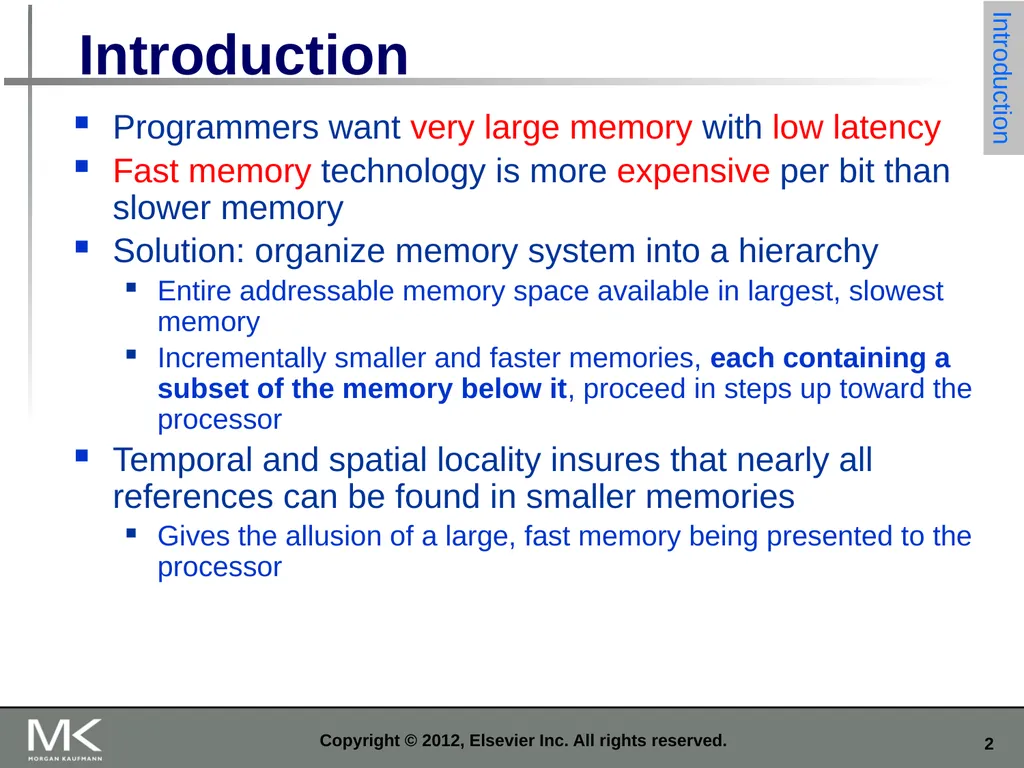
slide2. Copyright © 2012, Elsevier Inc. All rights reserved. Introduction Programmers want very large memory with low latency
Fast memory technology is more expensive per bit than slower memory
Solution: organize memory system into a hierarchy
Entire addressable memory space available in largest, slowest memory
Incrementally smaller and faster memories, each containing a subset of the memory below it, proceed in steps up toward the processor
Temporal and spatial locality insures that nearly all references can be found in smaller memories
Gives the allusion of a large, fast memory being presented to the processor Introduction<br>
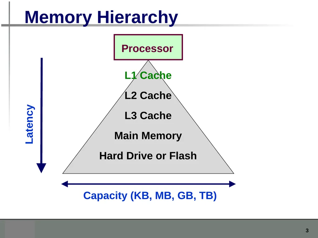
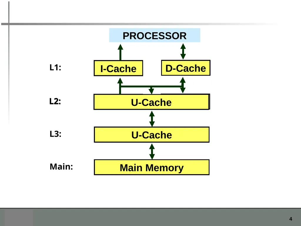
slide3. Memory Hierarchy Processor Latency L1 Cache
L2 Cache
L3 Cache
Main Memory
Hard Drive or Flash Capacity (KB, MB, GB, TB)<br>
slide4. PROCESSOR<br>
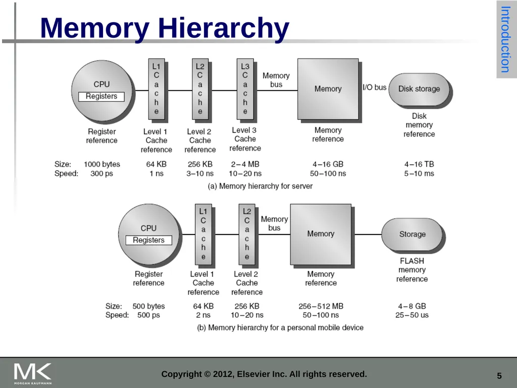
slide5. Copyright © 2012, Elsevier Inc. All rights reserved. Memory Hierarchy Introduction<br>
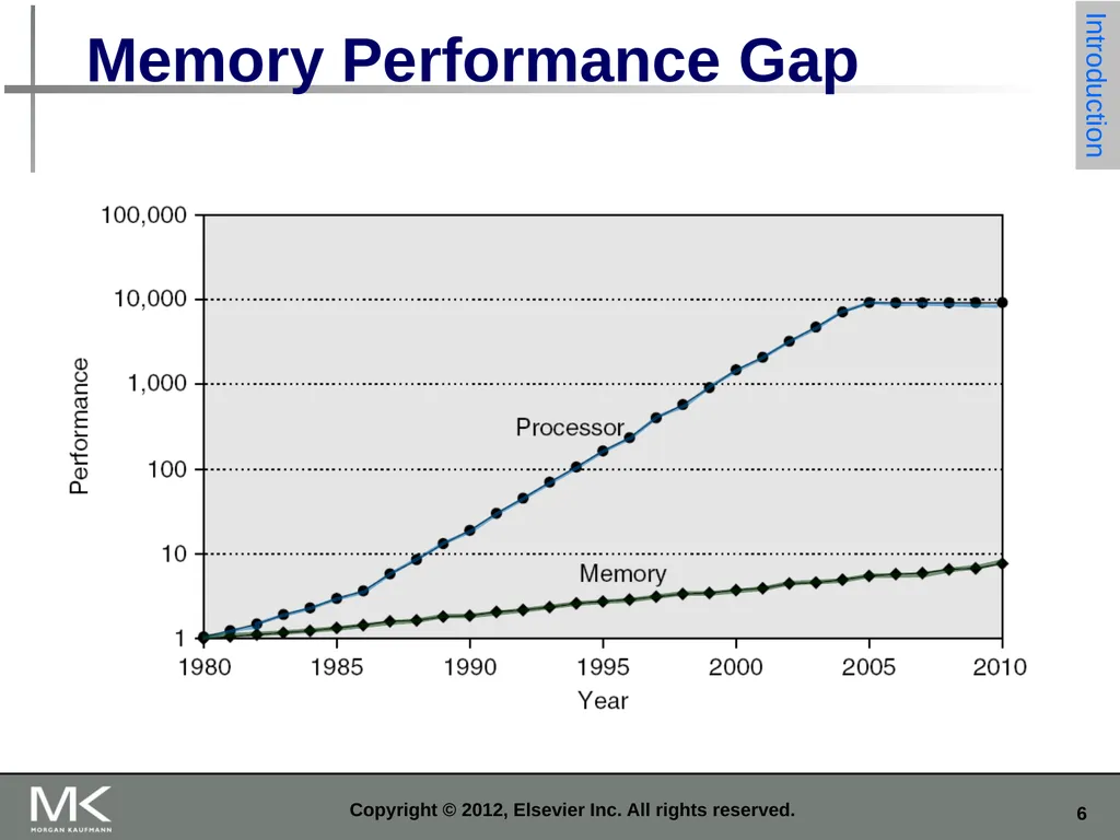
slide6. Copyright © 2012, Elsevier Inc. All rights reserved. Memory Performance Gap Introduction<br>
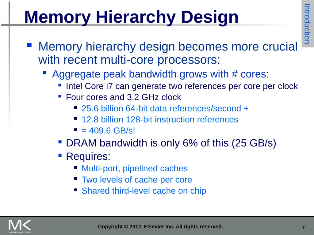
slide7. Copyright © 2012, Elsevier Inc. All rights reserved. Memory Hierarchy Design Memory hierarchy design becomes more crucial with recent multi-core processors:
Aggregate peak bandwidth grows with # cores:
Intel Core i7 can generate two references per core per clock
Four cores and 3.2 GHz clock
25.6 billion 64-bit data references/second +
12.8 billion 128-bit instruction references
= 409.6 GB/s!
DRAM bandwidth is only 6% of this (25 GB/s)
Requires:
Multi-port, pipelined caches
Two levels of cache per core
Shared third-level cache on chip Introduction<br>
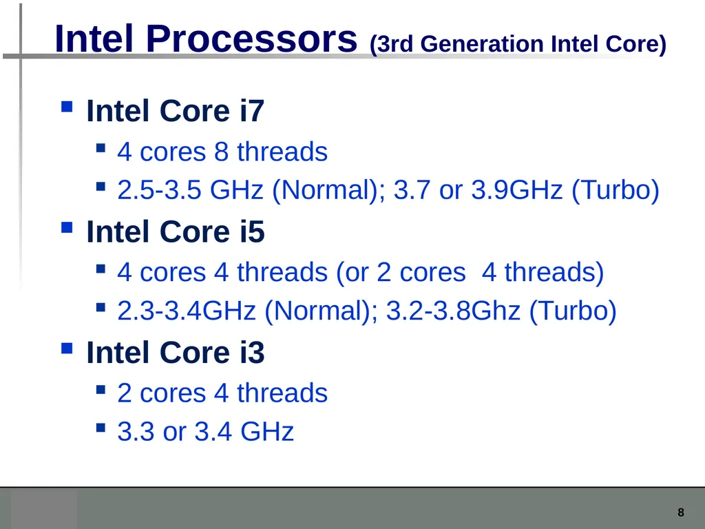
slide8. Intel Processors (3rd Generation Intel Core) Intel Core i7
4 cores 8 threads
2.5-3.5 GHz (Normal); 3.7 or 3.9GHz (Turbo)
Intel Core i5
4 cores 4 threads (or 2 cores 4 threads)
2.3-3.4GHz (Normal); 3.2-3.8Ghz (Turbo)
Intel Core i3
2 cores 4 threads
3.3 or 3.4 GHz<br>
slide9. Copyright © 2012, Elsevier Inc. All rights reserved. Performance and Power High-end microprocessors have >10 MB on-chip cache
Consumes large amount of area and power budget Introduction<br>
slide10. Copyright © 2012, Elsevier Inc. All rights reserved. Memory Hierarchy Basics When a word is not found in the cache, a miss occurs:
Fetch word from lower level in hierarchy, requiring a higher latency reference
Lower level may be another cache or the main memory
Also fetch the other words contained within the block
Takes advantage of spatial locality
Place block into cache in any location within its set, determined by address
block address MOD number of sets Introduction<br>
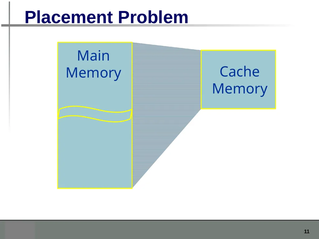
slide11. Placement Problem Main Memory Cache Memory<br>
slide12. Placement Policies WHERE to put a block in cache
Mapping between main and cache memories.
Main memory has a much larger capacity than cache memory.<br>
slide13. 0
1
2
3
4
5
6
7
8
9
10
11
12
13
14
15
16
17
18
19
20
21
22
23
24
25
26
27
28
29
30
31 Memory Block number 0
1
2
3
4
5
6
7 Fully Associative Cache Block can be placed in any location in cache.<br>
slide14. 0
1
2
3
4
5
6
7
8
9
10
11
12
13
14
15
16
17
18
19
20
21
22
23
24
25
26
27
28
29
30
31 Memory Block number 0
1
2
3
4
5
6
7 Direct Mapped Cache (Block address) MOD (Number of blocks in cache) 12 MOD 8 = 4 Block can be placed ONLY in a single location in cache.<br>
slide15. 0
1
2
3
4
5
6
7
8
9
10
11
12
13
14
15
16
17
18
19
20
21
22
23
24
25
26
27
28
29
30
31 Memory Block number 0
1
2
3
4
5
6
7 Set Associative Cache (Block address) MOD (Number of sets in cache) 12 MOD 4 = 0 0
1
2
3 Set no. Block number Block can be placed in one of n locations in n-way set associative cache.<br>
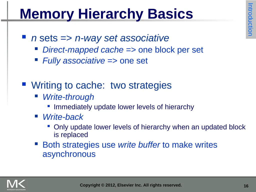
slide16. Copyright © 2012, Elsevier Inc. All rights reserved. Memory Hierarchy Basics n sets => n-way set associative
Direct-mapped cache => one block per set
Fully associative => one set
Writing to cache: two strategies
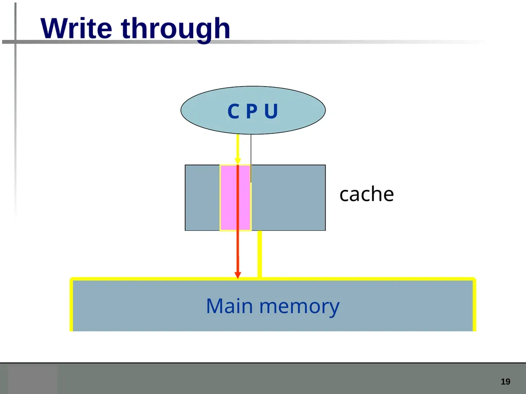
Write-through
Immediately update lower levels of hierarchy
Write-back
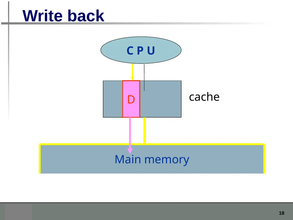
Only update lower levels of hierarchy when an updated block is replaced
Both strategies use write buffer to make writes asynchronous Introduction<br>
slide17. Dirty bit(s) Indicates if the block has been written to.
No need in I-caches.
No need in write through D-cache.
Write back D-cache needs it.<br>
slide18. Write back C P U Main memory cache D<br>
slide19. Write through C P U Main memory cache<br>
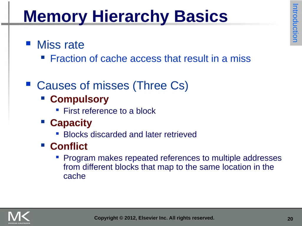
slide20. Copyright © 2012, Elsevier Inc. All rights reserved. Memory Hierarchy Basics Miss rate
Fraction of cache access that result in a miss
Causes of misses (Three Cs)
Compulsory
First reference to a block
Capacity
Blocks discarded and later retrieved
Conflict
Program makes repeated references to multiple addresses from different blocks that map to the same location in the cache Introduction<br>
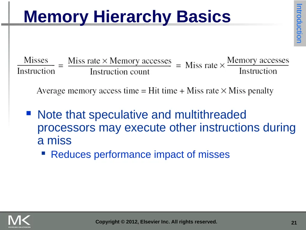
slide21. Note that speculative and multithreaded processors may execute other instructions during a miss
Reduces performance impact of misses Copyright © 2012, Elsevier Inc. All rights reserved. Memory Hierarchy Basics Introduction<br>
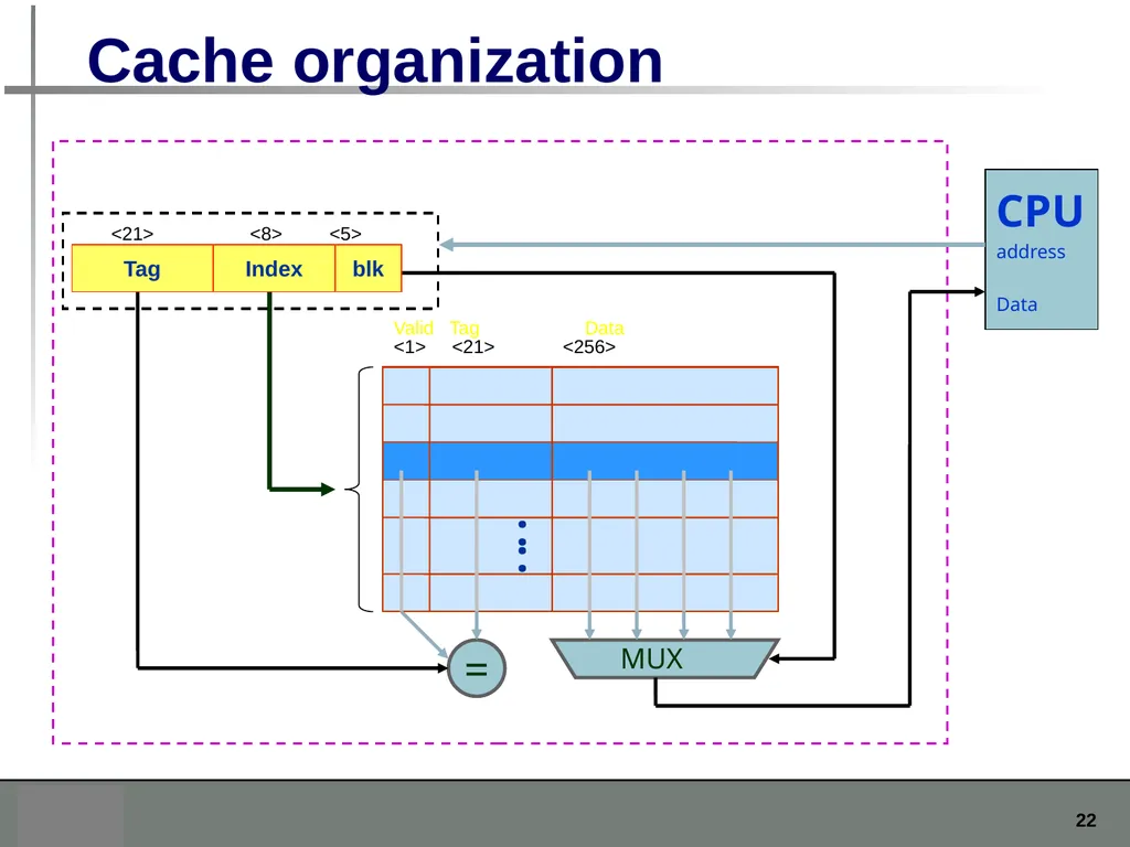
slide22. Cache organization <1> <21> <256> Valid Tag Data CPU
address
Data = MUX<br>
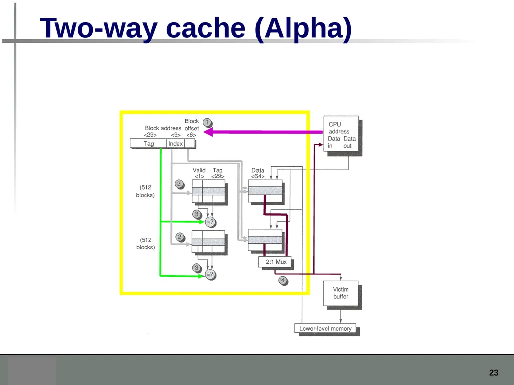
slide23. Two-way cache (Alpha)<br>
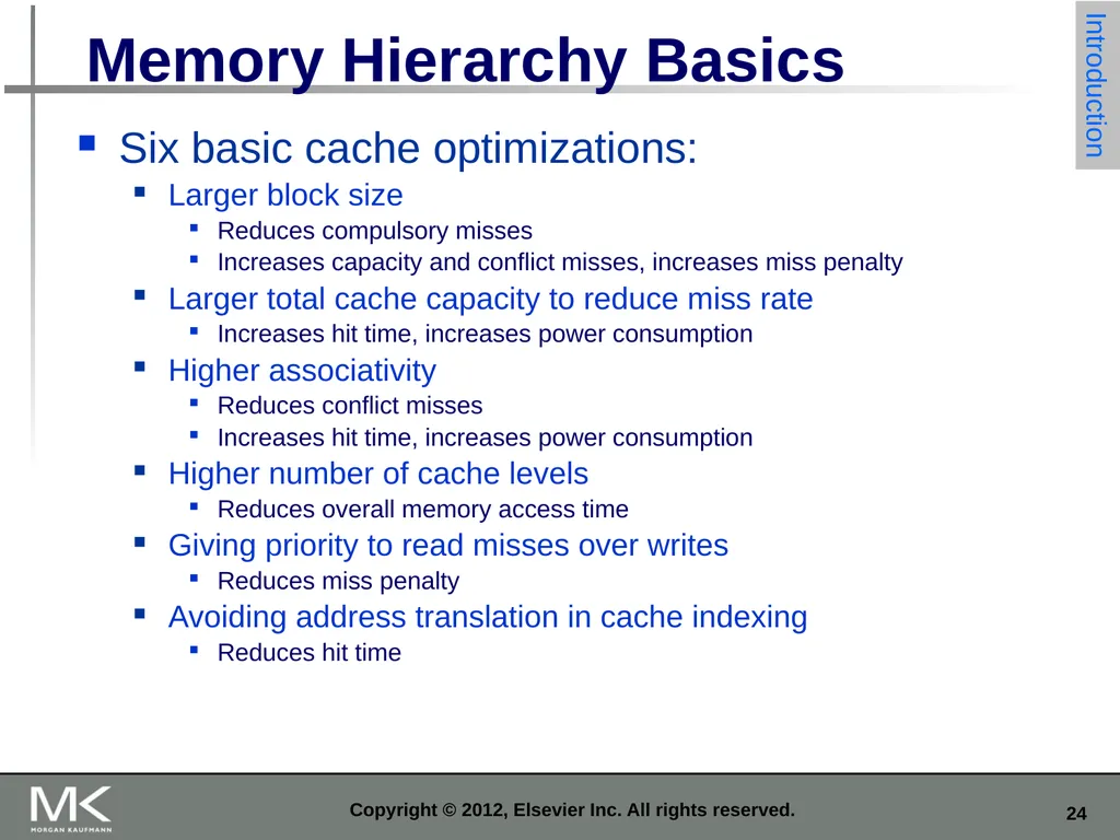
slide24. Copyright © 2012, Elsevier Inc. All rights reserved. Memory Hierarchy Basics Six basic cache optimizations:
Larger block size
Reduces compulsory misses
Increases capacity and conflict misses, increases miss penalty
Larger total cache capacity to reduce miss rate
Increases hit time, increases power consumption
Higher associativity
Reduces conflict misses
Increases hit time, increases power consumption
Higher number of cache levels
Reduces overall memory access time
Giving priority to read misses over writes
Reduces miss penalty
Avoiding address translation in cache indexing
Reduces hit time Introduction<br>
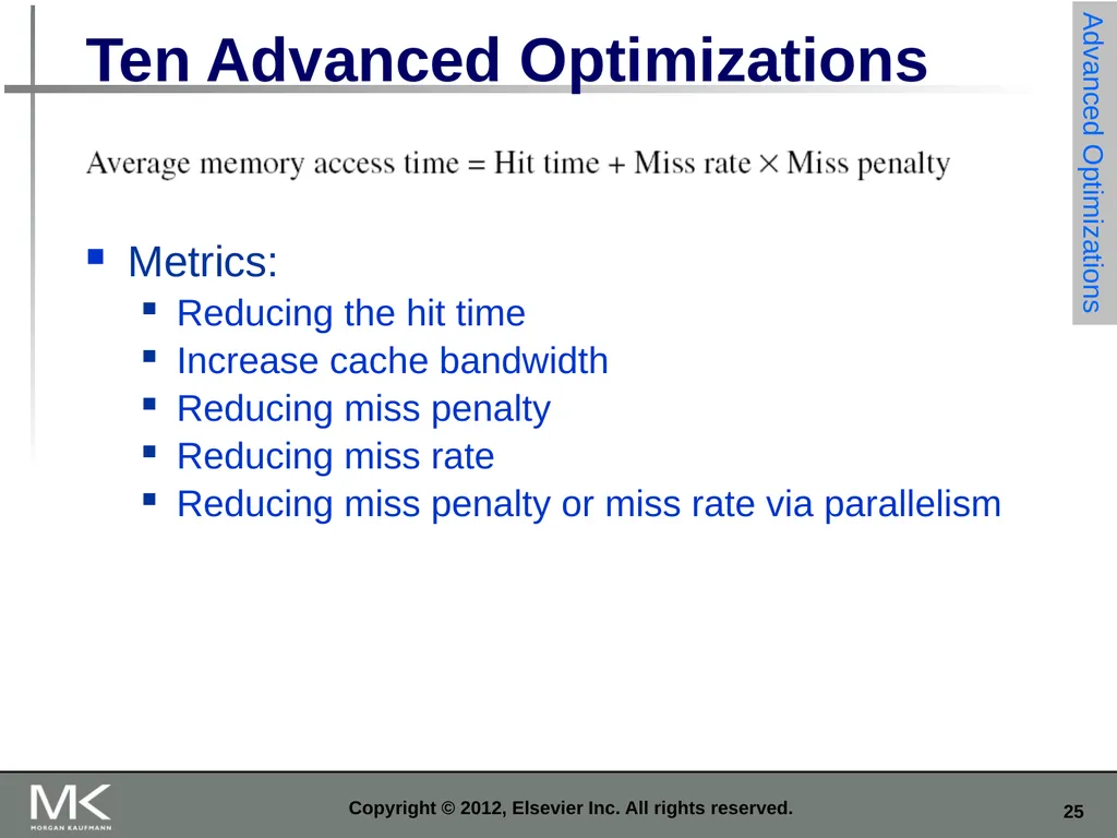
slide25. Copyright © 2012, Elsevier Inc. All rights reserved. Ten Advanced Optimizations Metrics:
Reducing the hit time
Increase cache bandwidth
Reducing miss penalty
Reducing miss rate
Reducing miss penalty or miss rate via parallelism Advanced Optimizations<br>
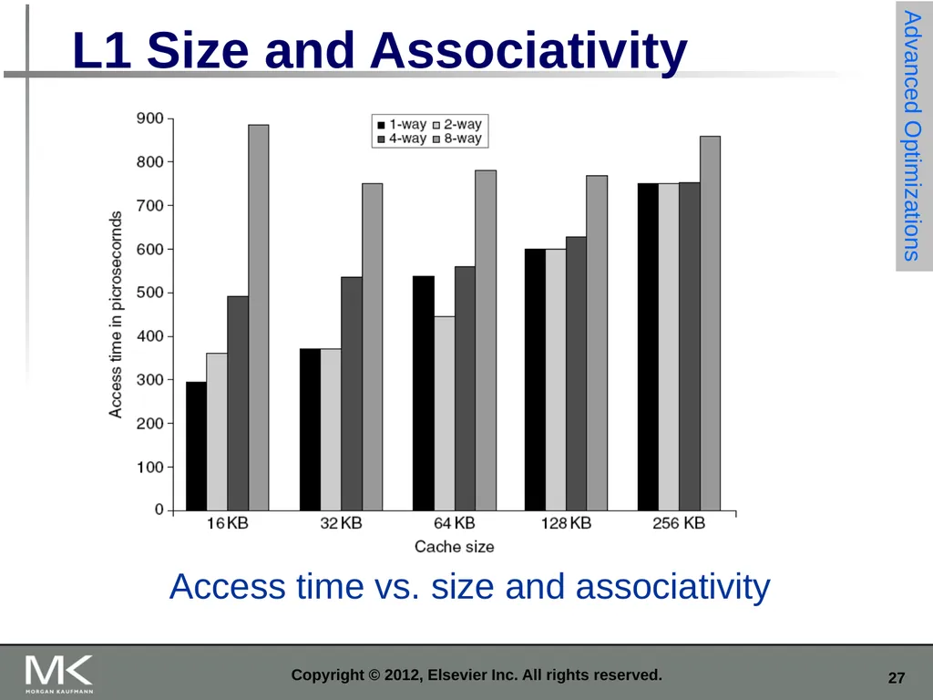
slide26. 1) Small and simple L1 caches Critical timing path:
addressing tag memory, then
comparing tags, then
selecting correct set
Direct-mapped caches can overlap tag compare and transmission of data
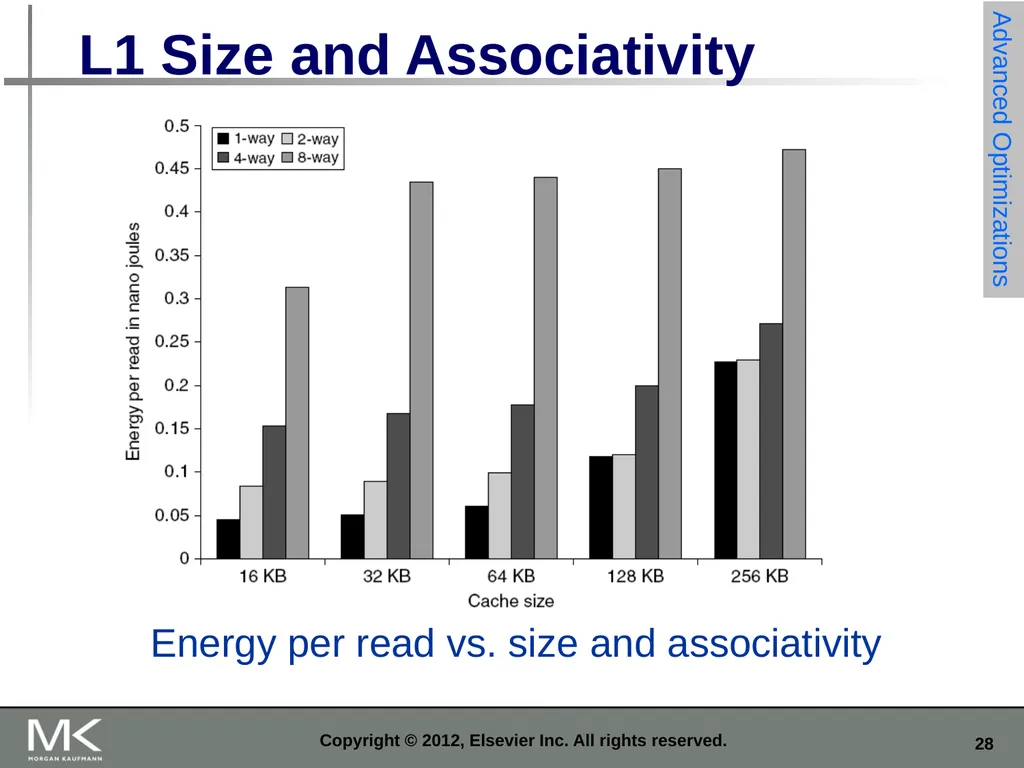
Lower associativity reduces power because fewer cache lines are accessed Copyright © 2012, Elsevier Inc. All rights reserved.<br>
slide27. Copyright © 2012, Elsevier Inc. All rights reserved. L1 Size and Associativity Access time vs. size and associativity Advanced Optimizations<br>
slide28. Copyright © 2012, Elsevier Inc. All rights reserved. L1 Size and Associativity Energy per read vs. size and associativity Advanced Optimizations<br>
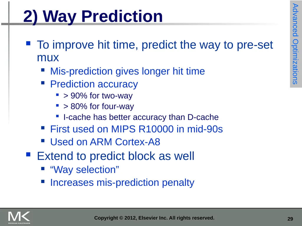
slide29. Copyright © 2012, Elsevier Inc. All rights reserved. 2) Way Prediction To improve hit time, predict the way to pre-set mux
Mis-prediction gives longer hit time
Prediction accuracy
> 90% for two-way
> 80% for four-way
I-cache has better accuracy than D-cache
First used on MIPS R10000 in mid-90s
Used on ARM Cortex-A8
Extend to predict block as well
“Way selection”
Increases mis-prediction penalty Advanced Optimizations<br>
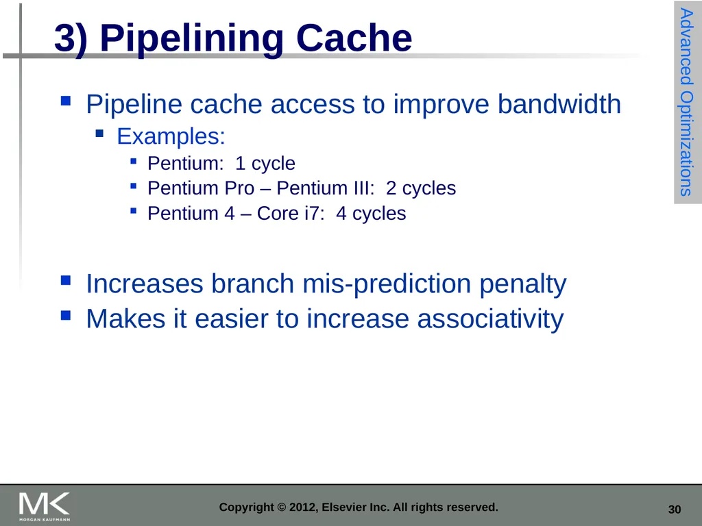
slide30. Copyright © 2012, Elsevier Inc. All rights reserved. 3) Pipelining Cache Pipeline cache access to improve bandwidth
Examples:
Pentium: 1 cycle
Pentium Pro – Pentium III: 2 cycles
Pentium 4 – Core i7: 4 cycles
Increases branch mis-prediction penalty
Makes it easier to increase associativity Advanced Optimizations<br>
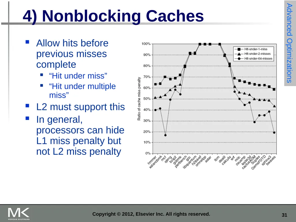
slide31. Copyright © 2012, Elsevier Inc. All rights reserved. 4) Nonblocking Caches Allow hits before previous misses complete
“Hit under miss”
“Hit under multiple miss”
L2 must support this
In general, processors can hide L1 miss penalty but not L2 miss penalty Advanced Optimizations<br>
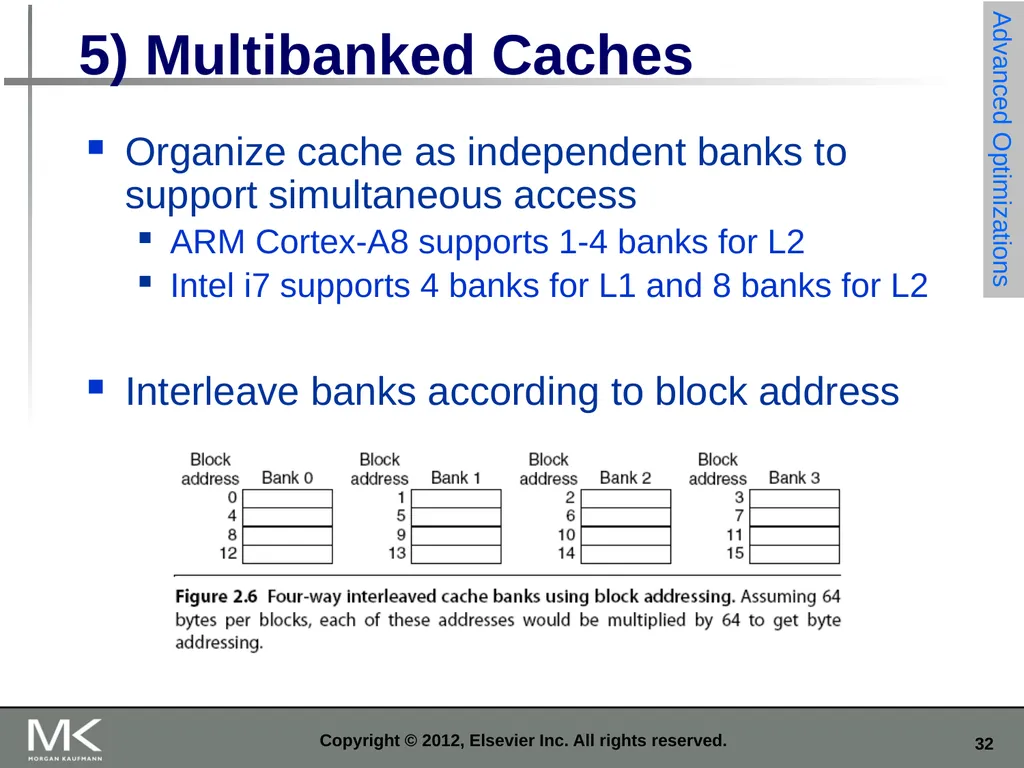
slide32. Copyright © 2012, Elsevier Inc. All rights reserved. 5) Multibanked Caches Organize cache as independent banks to support simultaneous access
ARM Cortex-A8 supports 1-4 banks for L2
Intel i7 supports 4 banks for L1 and 8 banks for L2
Interleave banks according to block address Advanced Optimizations<br>
slide33. Copyright © 2012, Elsevier Inc. All rights reserved. 6) Critical Word First, Early Restart Critical word first
Request missed word from memory first
Send it to the processor as soon as it arrives
Early restart
Request words in normal order
Send missed work to the processor as soon as it arrives
Effectiveness of these strategies depends on block size and likelihood of another access to the portion of the block that has not yet been fetched Advanced Optimizations<br>
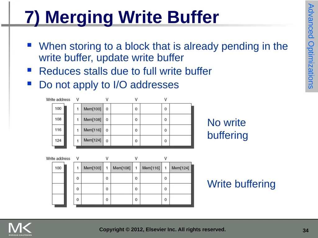
slide34. Copyright © 2012, Elsevier Inc. All rights reserved. 7) Merging Write Buffer When storing to a block that is already pending in the write buffer, update write buffer
Reduces stalls due to full write buffer
Do not apply to I/O addresses Advanced Optimizations No write buffering Write buffering<br>
slide35. Copyright © 2012, Elsevier Inc. All rights reserved. 8) Compiler Optimizations Loop Interchange
Swap nested loops to access memory in sequential order
Blocking
Instead of accessing entire rows or columns, subdivide matrices into blocks
Requires more memory accesses but improves locality of accesses Advanced Optimizations<br>
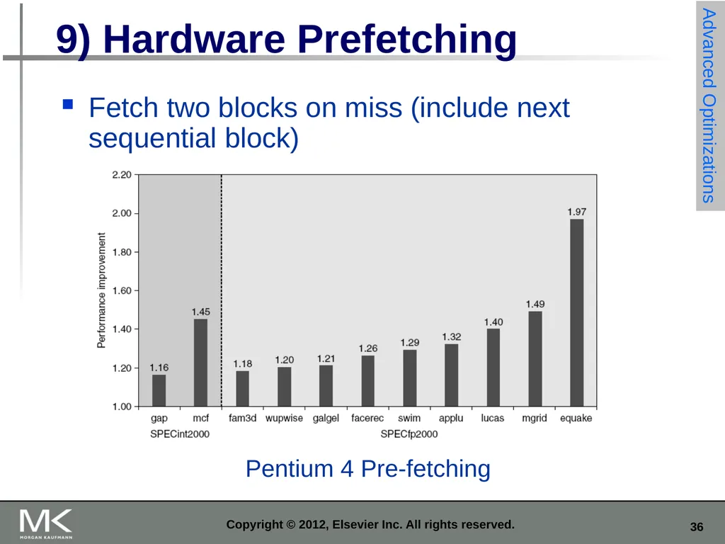
slide36. Copyright © 2012, Elsevier Inc. All rights reserved. 9) Hardware Prefetching Fetch two blocks on miss (include next sequential block) Advanced Optimizations Pentium 4 Pre-fetching<br>
slide37. Copyright © 2012, Elsevier Inc. All rights reserved. 10) Compiler Prefetching Insert prefetch instructions before data is needed
Non-faulting: prefetch doesn’t cause exceptions
Register prefetch
Loads data into register
Cache prefetch
Loads data into cache
Combine with loop unrolling and software pipelining Advanced Optimizations<br>
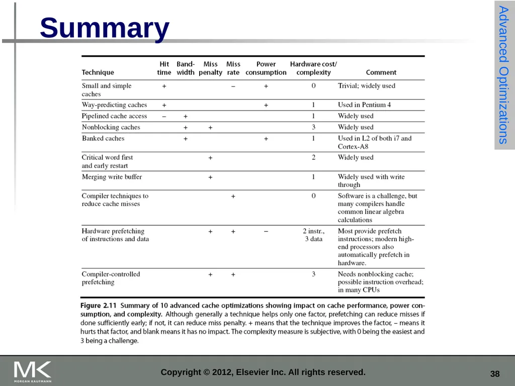
slide38. Copyright © 2012, Elsevier Inc. All rights reserved. Summary Advanced Optimizations<br>
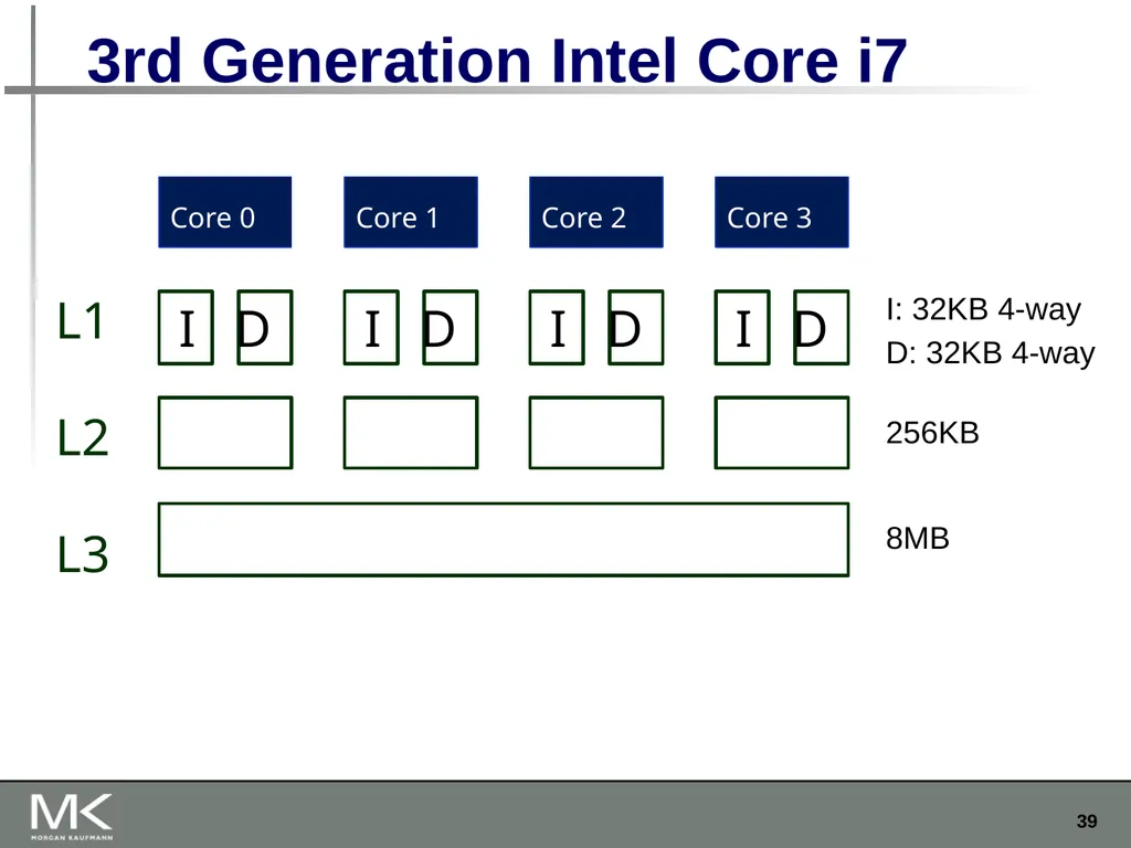
slide39. 3rd Generation Intel Core i7 Core 0 L1
L2
L3 I D Core 1 I D Core 2 I D Core 3 I D I: 32KB 4-way
D: 32KB 4-way 256KB 8MB<br>
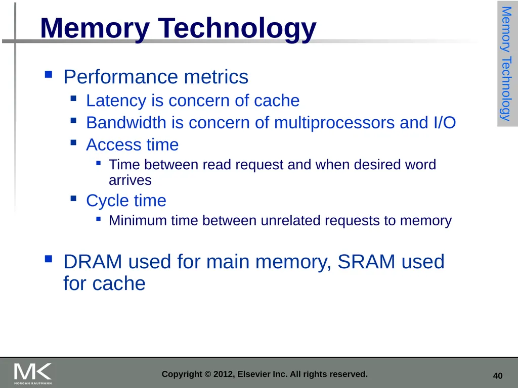
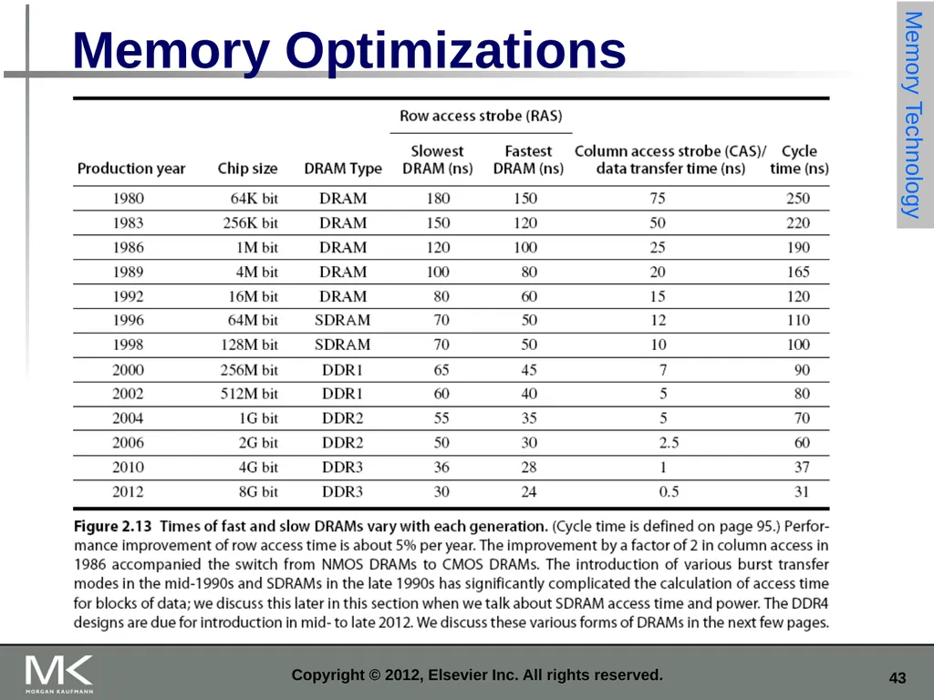
slide40. Copyright © 2012, Elsevier Inc. All rights reserved. Memory Technology Performance metrics
Latency is concern of cache
Bandwidth is concern of multiprocessors and I/O
Access time
Time between read request and when desired word arrives
Cycle time
Minimum time between unrelated requests to memory
DRAM used for main memory, SRAM used for cache Memory Technology<br>
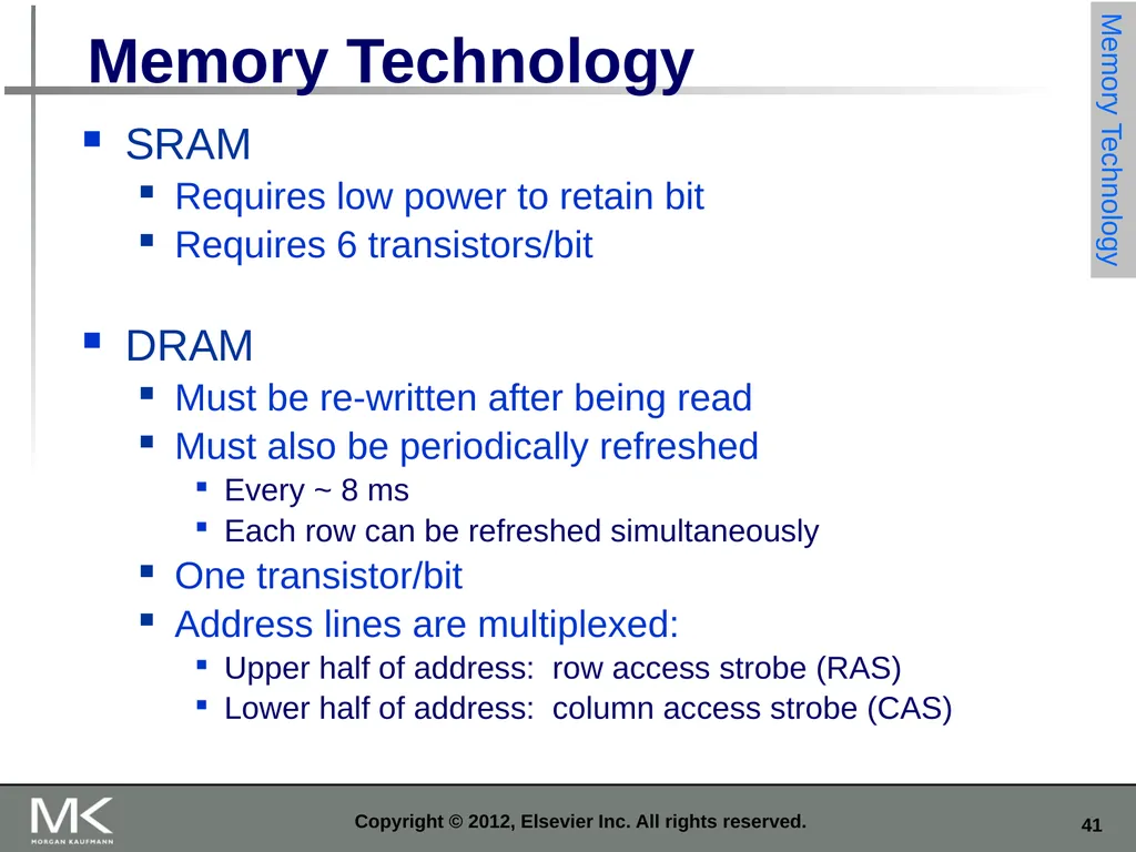
slide41. Copyright © 2012, Elsevier Inc. All rights reserved. Memory Technology SRAM
Requires low power to retain bit
Requires 6 transistors/bit
DRAM
Must be re-written after being read
Must also be periodically refreshed
Every ~ 8 ms
Each row can be refreshed simultaneously
One transistor/bit
Address lines are multiplexed:
Upper half of address: row access strobe (RAS)
Lower half of address: column access strobe (CAS) Memory Technology<br>
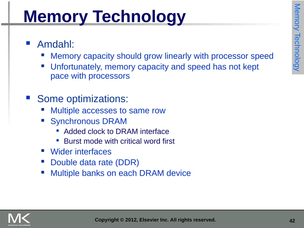
slide42. Copyright © 2012, Elsevier Inc. All rights reserved. Memory Technology Amdahl:
Memory capacity should grow linearly with processor speed
Unfortunately, memory capacity and speed has not kept pace with processors
Some optimizations:
Multiple accesses to same row
Synchronous DRAM
Added clock to DRAM interface
Burst mode with critical word first
Wider interfaces
Double data rate (DDR)
Multiple banks on each DRAM device Memory Technology<br>
slide43. Copyright © 2012, Elsevier Inc. All rights reserved. Memory Optimizations Memory Technology<br>
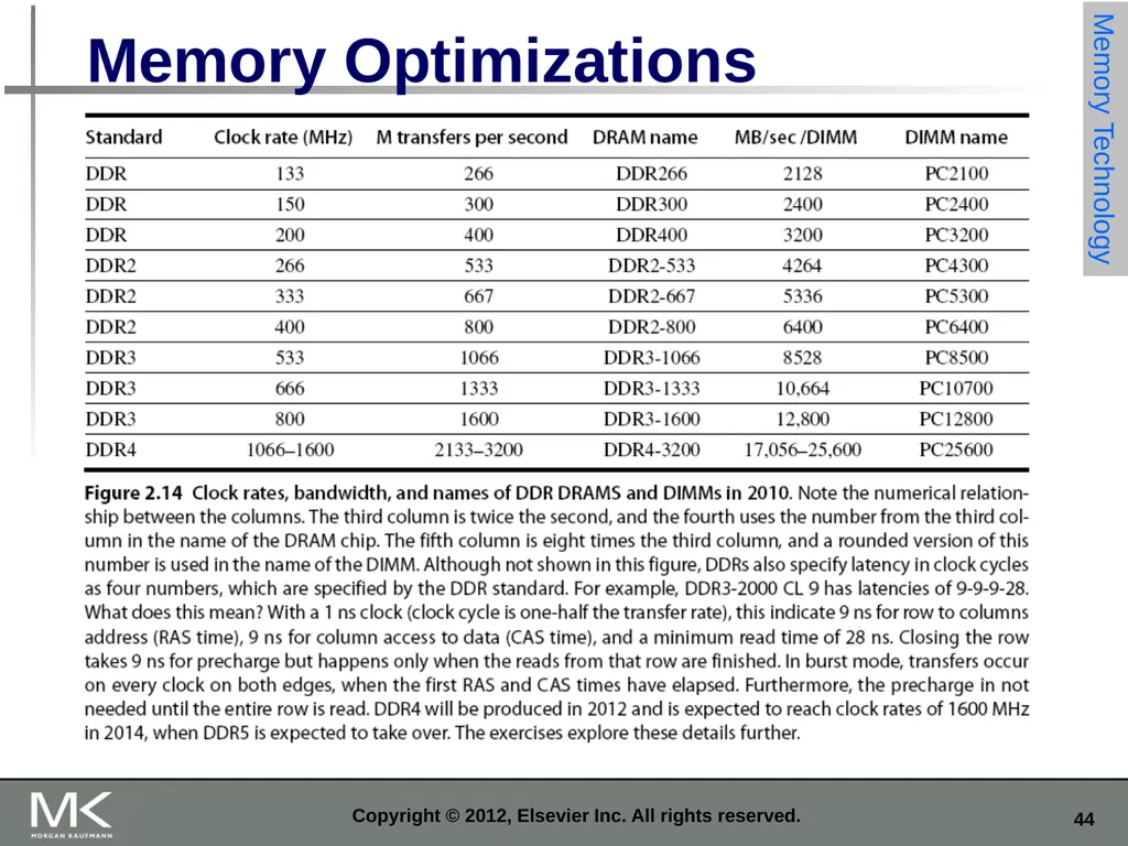
slide44. Copyright © 2012, Elsevier Inc. All rights reserved. Memory Optimizations Memory Technology<br>
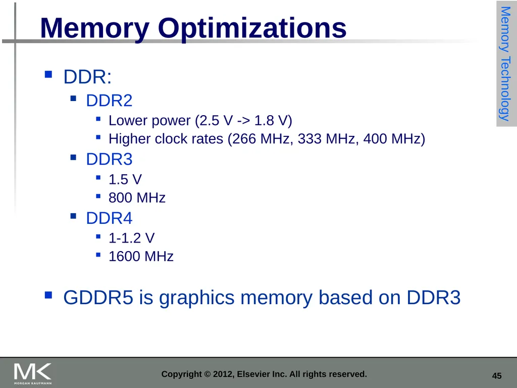
slide45. Copyright © 2012, Elsevier Inc. All rights reserved. Memory Optimizations DDR:
DDR2
Lower power (2.5 V -> 1.8 V)
Higher clock rates (266 MHz, 333 MHz, 400 MHz)
DDR3
1.5 V
800 MHz
DDR4
1-1.2 V
1600 MHz
GDDR5 is graphics memory based on DDR3 Memory Technology<br>
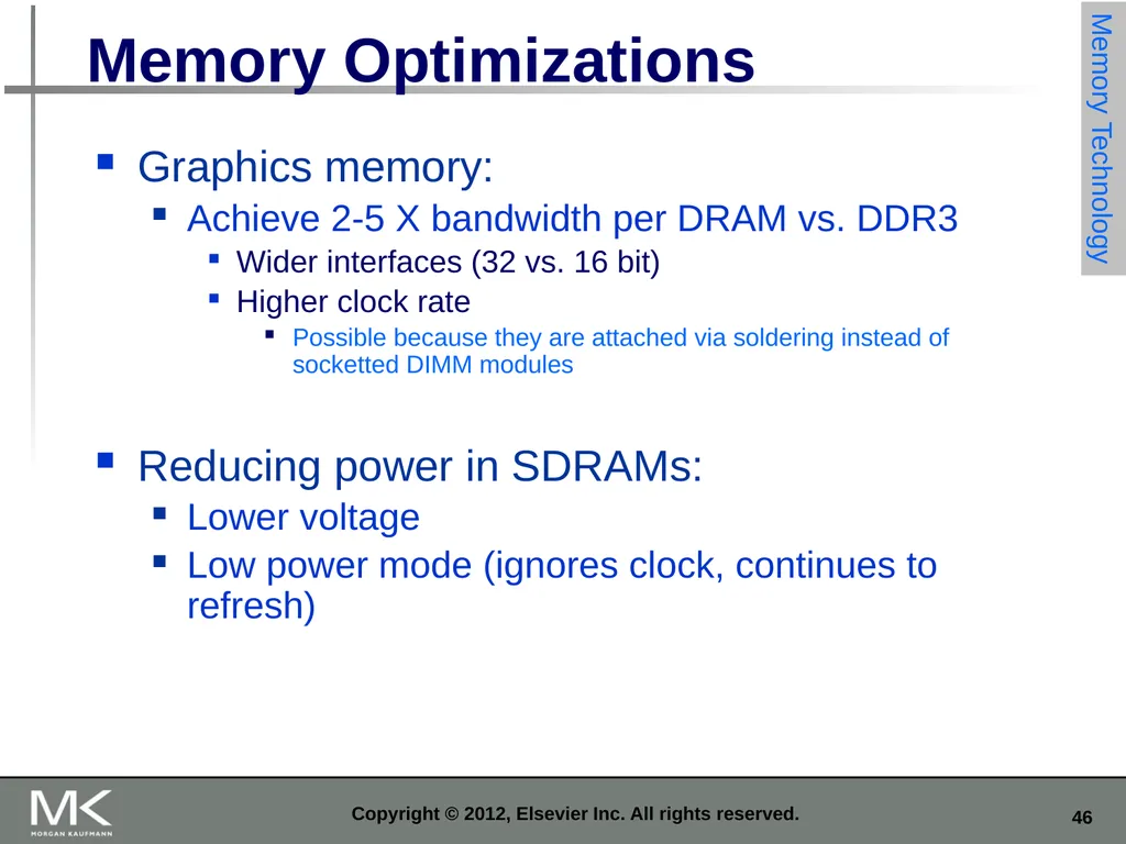
slide46. Copyright © 2012, Elsevier Inc. All rights reserved. Memory Optimizations Graphics memory:
Achieve 2-5 X bandwidth per DRAM vs. DDR3
Wider interfaces (32 vs. 16 bit)
Higher clock rate
Possible because they are attached via soldering instead of socketted DIMM modules
Reducing power in SDRAMs:
Lower voltage
Low power mode (ignores clock, continues to refresh) Memory Technology<br>
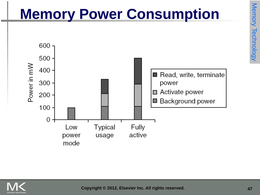
slide47. Copyright © 2012, Elsevier Inc. All rights reserved. Memory Power Consumption Memory Technology<br>
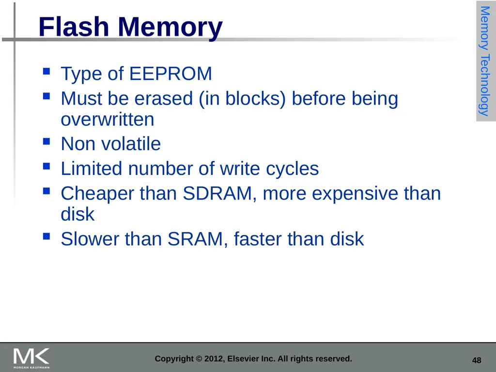
slide48. Copyright © 2012, Elsevier Inc. All rights reserved. Flash Memory Type of EEPROM
Must be erased (in blocks) before being overwritten
Non volatile
Limited number of write cycles
Cheaper than SDRAM, more expensive than disk
Slower than SRAM, faster than disk Memory Technology<br>
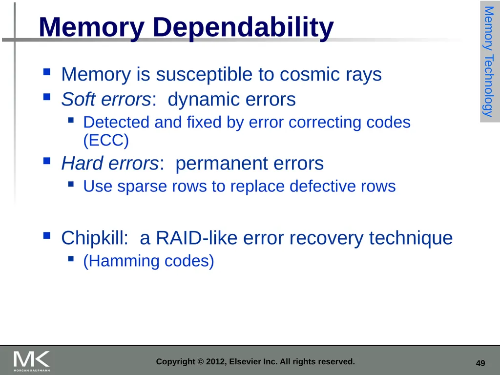
slide49. Copyright © 2012, Elsevier Inc. All rights reserved. Memory Dependability Memory is susceptible to cosmic rays
Soft errors: dynamic errors
Detected and fixed by error correcting codes (ECC)
Hard errors: permanent errors
Use sparse rows to replace defective rows
Chipkill: a RAID-like error recovery technique
(Hamming codes) Memory Technology<br>
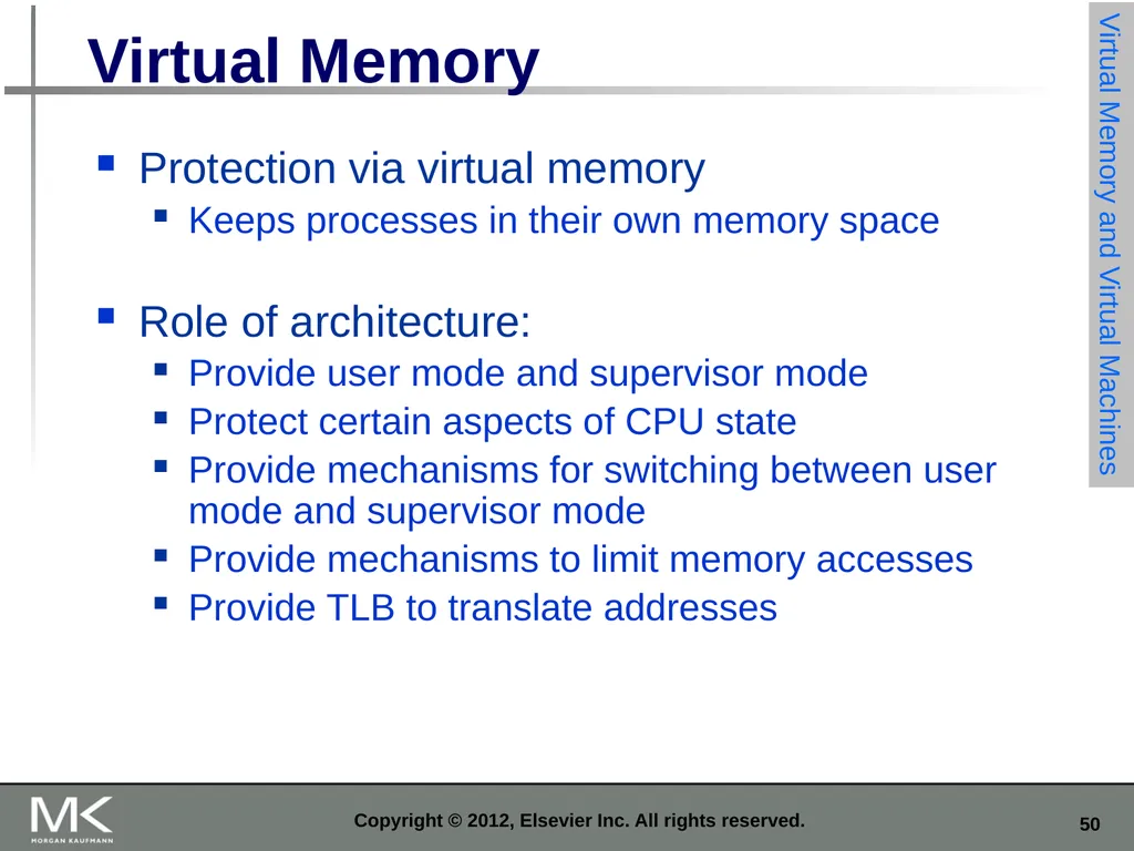
slide50. Copyright © 2012, Elsevier Inc. All rights reserved. Virtual Memory Protection via virtual memory
Keeps processes in their own memory space
Role of architecture:
Provide user mode and supervisor mode
Protect certain aspects of CPU state
Provide mechanisms for switching between user mode and supervisor mode
Provide mechanisms to limit memory accesses
Provide TLB to translate addresses Virtual Memory and Virtual Machines<br>
slide51. Copyright © 2012, Elsevier Inc. All rights reserved. Virtual Machines Supports isolation and security
Sharing a computer among many unrelated users
Enabled by raw speed of processors, making the overhead more acceptable
Allows different ISAs and operating systems to be presented to user programs
“System Virtual Machines”
SVM software is called “virtual machine monitor” or “hypervisor”
Individual virtual machines run under the monitor are called “guest VMs” Virtual Memory and Virtual Machines<br>
slide52. Copyright © 2012, Elsevier Inc. All rights reserved. Impact of VMs on Virtual Memory Each guest OS maintains its own set of page tables
VMM adds a level of memory between physical and virtual memory called “real memory”
VMM maintains shadow page table that maps guest virtual addresses to physical addresses
Requires VMM to detect guest’s changes to its own page table
Occurs naturally if accessing the page table pointer is a privileged operation Virtual Memory and Virtual Machines<br>
A Quantitative Approach, Fifth Edition<br>
slide2. Copyright © 2012, Elsevier Inc. All rights reserved. Introduction Programmers want very large memory with low latency
Fast memory technology is more expensive per bit than slower memory
Solution: organize memory system into a hierarchy
Entire addressable memory space available in largest, slowest memory
Incrementally smaller and faster memories, each containing a subset of the memory below it, proceed in steps up toward the processor
Temporal and spatial locality insures that nearly all references can be found in smaller memories
Gives the allusion of a large, fast memory being presented to the processor Introduction<br>
slide3. Memory Hierarchy Processor Latency L1 Cache
L2 Cache
L3 Cache
Main Memory
Hard Drive or Flash Capacity (KB, MB, GB, TB)<br>
slide4. PROCESSOR<br>
slide5. Copyright © 2012, Elsevier Inc. All rights reserved. Memory Hierarchy Introduction<br>
slide6. Copyright © 2012, Elsevier Inc. All rights reserved. Memory Performance Gap Introduction<br>
slide7. Copyright © 2012, Elsevier Inc. All rights reserved. Memory Hierarchy Design Memory hierarchy design becomes more crucial with recent multi-core processors:
Aggregate peak bandwidth grows with # cores:
Intel Core i7 can generate two references per core per clock
Four cores and 3.2 GHz clock
25.6 billion 64-bit data references/second +
12.8 billion 128-bit instruction references
= 409.6 GB/s!
DRAM bandwidth is only 6% of this (25 GB/s)
Requires:
Multi-port, pipelined caches
Two levels of cache per core
Shared third-level cache on chip Introduction<br>
slide8. Intel Processors (3rd Generation Intel Core) Intel Core i7
4 cores 8 threads
2.5-3.5 GHz (Normal); 3.7 or 3.9GHz (Turbo)
Intel Core i5
4 cores 4 threads (or 2 cores 4 threads)
2.3-3.4GHz (Normal); 3.2-3.8Ghz (Turbo)
Intel Core i3
2 cores 4 threads
3.3 or 3.4 GHz<br>
slide9. Copyright © 2012, Elsevier Inc. All rights reserved. Performance and Power High-end microprocessors have >10 MB on-chip cache
Consumes large amount of area and power budget Introduction<br>
slide10. Copyright © 2012, Elsevier Inc. All rights reserved. Memory Hierarchy Basics When a word is not found in the cache, a miss occurs:
Fetch word from lower level in hierarchy, requiring a higher latency reference
Lower level may be another cache or the main memory
Also fetch the other words contained within the block
Takes advantage of spatial locality
Place block into cache in any location within its set, determined by address
block address MOD number of sets Introduction<br>
slide11. Placement Problem Main Memory Cache Memory<br>
slide12. Placement Policies WHERE to put a block in cache
Mapping between main and cache memories.
Main memory has a much larger capacity than cache memory.<br>
slide13. 0
1
2
3
4
5
6
7
8
9
10
11
12
13
14
15
16
17
18
19
20
21
22
23
24
25
26
27
28
29
30
31 Memory Block number 0
1
2
3
4
5
6
7 Fully Associative Cache Block can be placed in any location in cache.<br>
slide14. 0
1
2
3
4
5
6
7
8
9
10
11
12
13
14
15
16
17
18
19
20
21
22
23
24
25
26
27
28
29
30
31 Memory Block number 0
1
2
3
4
5
6
7 Direct Mapped Cache (Block address) MOD (Number of blocks in cache) 12 MOD 8 = 4 Block can be placed ONLY in a single location in cache.<br>
slide15. 0
1
2
3
4
5
6
7
8
9
10
11
12
13
14
15
16
17
18
19
20
21
22
23
24
25
26
27
28
29
30
31 Memory Block number 0
1
2
3
4
5
6
7 Set Associative Cache (Block address) MOD (Number of sets in cache) 12 MOD 4 = 0 0
1
2
3 Set no. Block number Block can be placed in one of n locations in n-way set associative cache.<br>
slide16. Copyright © 2012, Elsevier Inc. All rights reserved. Memory Hierarchy Basics n sets => n-way set associative
Direct-mapped cache => one block per set
Fully associative => one set
Writing to cache: two strategies
Write-through
Immediately update lower levels of hierarchy
Write-back
Only update lower levels of hierarchy when an updated block is replaced
Both strategies use write buffer to make writes asynchronous Introduction<br>
slide17. Dirty bit(s) Indicates if the block has been written to.
No need in I-caches.
No need in write through D-cache.
Write back D-cache needs it.<br>
slide18. Write back C P U Main memory cache D<br>
slide19. Write through C P U Main memory cache<br>
slide20. Copyright © 2012, Elsevier Inc. All rights reserved. Memory Hierarchy Basics Miss rate
Fraction of cache access that result in a miss
Causes of misses (Three Cs)
Compulsory
First reference to a block
Capacity
Blocks discarded and later retrieved
Conflict
Program makes repeated references to multiple addresses from different blocks that map to the same location in the cache Introduction<br>
slide21. Note that speculative and multithreaded processors may execute other instructions during a miss
Reduces performance impact of misses Copyright © 2012, Elsevier Inc. All rights reserved. Memory Hierarchy Basics Introduction<br>
slide22. Cache organization <1> <21> <256> Valid Tag Data CPU
address
Data = MUX<br>
slide23. Two-way cache (Alpha)<br>
slide24. Copyright © 2012, Elsevier Inc. All rights reserved. Memory Hierarchy Basics Six basic cache optimizations:
Larger block size
Reduces compulsory misses
Increases capacity and conflict misses, increases miss penalty
Larger total cache capacity to reduce miss rate
Increases hit time, increases power consumption
Higher associativity
Reduces conflict misses
Increases hit time, increases power consumption
Higher number of cache levels
Reduces overall memory access time
Giving priority to read misses over writes
Reduces miss penalty
Avoiding address translation in cache indexing
Reduces hit time Introduction<br>
slide25. Copyright © 2012, Elsevier Inc. All rights reserved. Ten Advanced Optimizations Metrics:
Reducing the hit time
Increase cache bandwidth
Reducing miss penalty
Reducing miss rate
Reducing miss penalty or miss rate via parallelism Advanced Optimizations<br>
slide26. 1) Small and simple L1 caches Critical timing path:
addressing tag memory, then
comparing tags, then
selecting correct set
Direct-mapped caches can overlap tag compare and transmission of data
Lower associativity reduces power because fewer cache lines are accessed Copyright © 2012, Elsevier Inc. All rights reserved.<br>
slide27. Copyright © 2012, Elsevier Inc. All rights reserved. L1 Size and Associativity Access time vs. size and associativity Advanced Optimizations<br>
slide28. Copyright © 2012, Elsevier Inc. All rights reserved. L1 Size and Associativity Energy per read vs. size and associativity Advanced Optimizations<br>
slide29. Copyright © 2012, Elsevier Inc. All rights reserved. 2) Way Prediction To improve hit time, predict the way to pre-set mux
Mis-prediction gives longer hit time
Prediction accuracy
> 90% for two-way
> 80% for four-way
I-cache has better accuracy than D-cache
First used on MIPS R10000 in mid-90s
Used on ARM Cortex-A8
Extend to predict block as well
“Way selection”
Increases mis-prediction penalty Advanced Optimizations<br>
slide30. Copyright © 2012, Elsevier Inc. All rights reserved. 3) Pipelining Cache Pipeline cache access to improve bandwidth
Examples:
Pentium: 1 cycle
Pentium Pro – Pentium III: 2 cycles
Pentium 4 – Core i7: 4 cycles
Increases branch mis-prediction penalty
Makes it easier to increase associativity Advanced Optimizations<br>
slide31. Copyright © 2012, Elsevier Inc. All rights reserved. 4) Nonblocking Caches Allow hits before previous misses complete
“Hit under miss”
“Hit under multiple miss”
L2 must support this
In general, processors can hide L1 miss penalty but not L2 miss penalty Advanced Optimizations<br>
slide32. Copyright © 2012, Elsevier Inc. All rights reserved. 5) Multibanked Caches Organize cache as independent banks to support simultaneous access
ARM Cortex-A8 supports 1-4 banks for L2
Intel i7 supports 4 banks for L1 and 8 banks for L2
Interleave banks according to block address Advanced Optimizations<br>
slide33. Copyright © 2012, Elsevier Inc. All rights reserved. 6) Critical Word First, Early Restart Critical word first
Request missed word from memory first
Send it to the processor as soon as it arrives
Early restart
Request words in normal order
Send missed work to the processor as soon as it arrives
Effectiveness of these strategies depends on block size and likelihood of another access to the portion of the block that has not yet been fetched Advanced Optimizations<br>
slide34. Copyright © 2012, Elsevier Inc. All rights reserved. 7) Merging Write Buffer When storing to a block that is already pending in the write buffer, update write buffer
Reduces stalls due to full write buffer
Do not apply to I/O addresses Advanced Optimizations No write buffering Write buffering<br>
slide35. Copyright © 2012, Elsevier Inc. All rights reserved. 8) Compiler Optimizations Loop Interchange
Swap nested loops to access memory in sequential order
Blocking
Instead of accessing entire rows or columns, subdivide matrices into blocks
Requires more memory accesses but improves locality of accesses Advanced Optimizations<br>
slide36. Copyright © 2012, Elsevier Inc. All rights reserved. 9) Hardware Prefetching Fetch two blocks on miss (include next sequential block) Advanced Optimizations Pentium 4 Pre-fetching<br>
slide37. Copyright © 2012, Elsevier Inc. All rights reserved. 10) Compiler Prefetching Insert prefetch instructions before data is needed
Non-faulting: prefetch doesn’t cause exceptions
Register prefetch
Loads data into register
Cache prefetch
Loads data into cache
Combine with loop unrolling and software pipelining Advanced Optimizations<br>
slide38. Copyright © 2012, Elsevier Inc. All rights reserved. Summary Advanced Optimizations<br>
slide39. 3rd Generation Intel Core i7 Core 0 L1
L2
L3 I D Core 1 I D Core 2 I D Core 3 I D I: 32KB 4-way
D: 32KB 4-way 256KB 8MB<br>
slide40. Copyright © 2012, Elsevier Inc. All rights reserved. Memory Technology Performance metrics
Latency is concern of cache
Bandwidth is concern of multiprocessors and I/O
Access time
Time between read request and when desired word arrives
Cycle time
Minimum time between unrelated requests to memory
DRAM used for main memory, SRAM used for cache Memory Technology<br>
slide41. Copyright © 2012, Elsevier Inc. All rights reserved. Memory Technology SRAM
Requires low power to retain bit
Requires 6 transistors/bit
DRAM
Must be re-written after being read
Must also be periodically refreshed
Every ~ 8 ms
Each row can be refreshed simultaneously
One transistor/bit
Address lines are multiplexed:
Upper half of address: row access strobe (RAS)
Lower half of address: column access strobe (CAS) Memory Technology<br>
slide42. Copyright © 2012, Elsevier Inc. All rights reserved. Memory Technology Amdahl:
Memory capacity should grow linearly with processor speed
Unfortunately, memory capacity and speed has not kept pace with processors
Some optimizations:
Multiple accesses to same row
Synchronous DRAM
Added clock to DRAM interface
Burst mode with critical word first
Wider interfaces
Double data rate (DDR)
Multiple banks on each DRAM device Memory Technology<br>
slide43. Copyright © 2012, Elsevier Inc. All rights reserved. Memory Optimizations Memory Technology<br>
slide44. Copyright © 2012, Elsevier Inc. All rights reserved. Memory Optimizations Memory Technology<br>
slide45. Copyright © 2012, Elsevier Inc. All rights reserved. Memory Optimizations DDR:
DDR2
Lower power (2.5 V -> 1.8 V)
Higher clock rates (266 MHz, 333 MHz, 400 MHz)
DDR3
1.5 V
800 MHz
DDR4
1-1.2 V
1600 MHz
GDDR5 is graphics memory based on DDR3 Memory Technology<br>
slide46. Copyright © 2012, Elsevier Inc. All rights reserved. Memory Optimizations Graphics memory:
Achieve 2-5 X bandwidth per DRAM vs. DDR3
Wider interfaces (32 vs. 16 bit)
Higher clock rate
Possible because they are attached via soldering instead of socketted DIMM modules
Reducing power in SDRAMs:
Lower voltage
Low power mode (ignores clock, continues to refresh) Memory Technology<br>
slide47. Copyright © 2012, Elsevier Inc. All rights reserved. Memory Power Consumption Memory Technology<br>
slide48. Copyright © 2012, Elsevier Inc. All rights reserved. Flash Memory Type of EEPROM
Must be erased (in blocks) before being overwritten
Non volatile
Limited number of write cycles
Cheaper than SDRAM, more expensive than disk
Slower than SRAM, faster than disk Memory Technology<br>
slide49. Copyright © 2012, Elsevier Inc. All rights reserved. Memory Dependability Memory is susceptible to cosmic rays
Soft errors: dynamic errors
Detected and fixed by error correcting codes (ECC)
Hard errors: permanent errors
Use sparse rows to replace defective rows
Chipkill: a RAID-like error recovery technique
(Hamming codes) Memory Technology<br>
slide50. Copyright © 2012, Elsevier Inc. All rights reserved. Virtual Memory Protection via virtual memory
Keeps processes in their own memory space
Role of architecture:
Provide user mode and supervisor mode
Protect certain aspects of CPU state
Provide mechanisms for switching between user mode and supervisor mode
Provide mechanisms to limit memory accesses
Provide TLB to translate addresses Virtual Memory and Virtual Machines<br>
slide51. Copyright © 2012, Elsevier Inc. All rights reserved. Virtual Machines Supports isolation and security
Sharing a computer among many unrelated users
Enabled by raw speed of processors, making the overhead more acceptable
Allows different ISAs and operating systems to be presented to user programs
“System Virtual Machines”
SVM software is called “virtual machine monitor” or “hypervisor”
Individual virtual machines run under the monitor are called “guest VMs” Virtual Memory and Virtual Machines<br>
slide52. Copyright © 2012, Elsevier Inc. All rights reserved. Impact of VMs on Virtual Memory Each guest OS maintains its own set of page tables
VMM adds a level of memory between physical and virtual memory called “real memory”
VMM maintains shadow page table that maps guest virtual addresses to physical addresses
Requires VMM to detect guest’s changes to its own page table
Occurs naturally if accessing the page table pointer is a privileged operation Virtual Memory and Virtual Machines<br>