Dedicated logic circuits Technological solutions
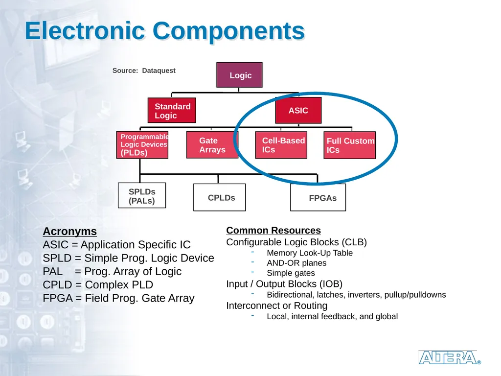
Description: Dedicated logic circuits Technological solutions Electronic Components Source: Dataquest Programmable Logic Devices (PLDs) Gate Arrays Cell-Based ICs Full Custom ICs SPLDs (PALs) FPGAs Acronyms ASIC Application Specific IC SPLD Simple
Related Topics
Download Presentation
"Dedicated logic circuits Technological solutions" is the property of its rightful owner. Permission is granted to download and print the materials on this website for personal, non-commercial use only, and to display it on your personal computer provided you do not modify the materials and that you retain all copyright notices contained in the materials. By downloading content from our website, you accept the terms of this agreement.
Presentation Transcript
slide1. Dedicated logic circuits Technological solutions<br>
slide2. Electronic Components Source: Dataquest Programmable
Logic Devices
(PLDs) Gate
Arrays Cell-Based
ICs Full Custom
ICs SPLDs
(PALs) FPGAs Acronyms
ASIC = Application Specific IC
SPLD = Simple Prog. Logic Device
PAL = Prog. Array of Logic
CPLD = Complex PLD
FPGA = Field Prog. Gate Array Common Resources
Configurable Logic Blocks (CLB)
Memory Look-Up Table
AND-OR planes
Simple gates
Input / Output Blocks (IOB)
Bidirectional, latches, inverters, pullup/pulldowns
Interconnect or Routing
Local, internal feedback, and global<br>
slide3. Key parameters Number of pieces to be produced
Cost of the prototype
Cost of the chip in production
Performance:
Occupied area
Working frequency
Power dissipation
Time to Market<br>
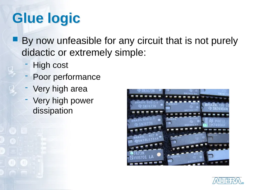
slide4. Glue logic By now unfeasible for any circuit that is not purely didactic or extremely simple:
High cost
Poor performance
Very high area
Very high power dissipation<br>
slide5. Full Custom Great performance
Very high prototype cost
Low cost for mass production
Very complex and laborious project (requires a group of specialists occupied for some time)
Long times before having the finished product:
Project
Passage through the foundry
Testing<br>
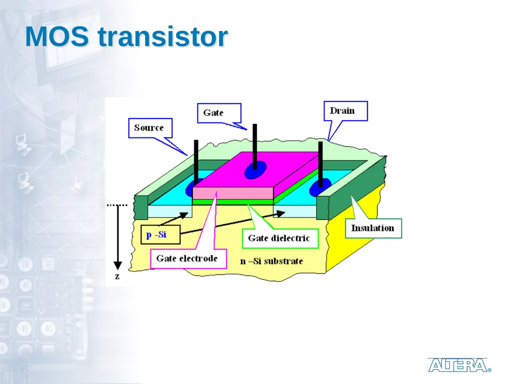
slide6. MOS transistor<br>
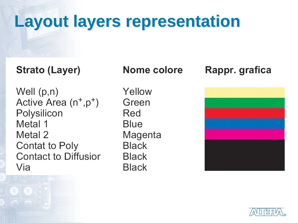
slide7. Layout layers representation<br>
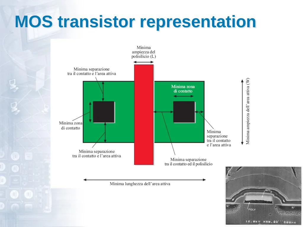
slide8. MOS transistor representation<br>
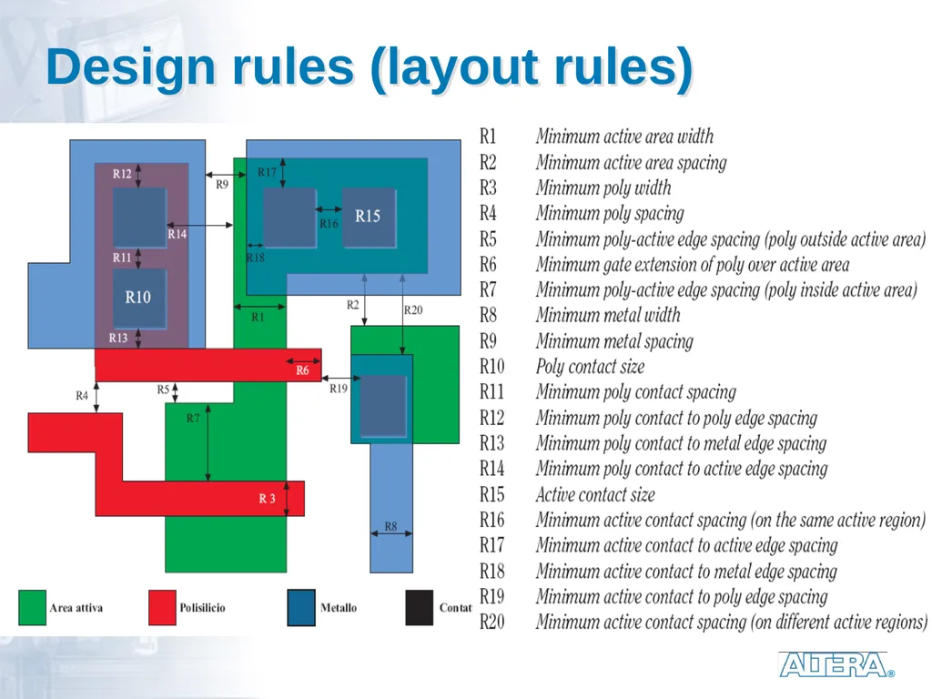
slide9. Design rules (layout rules)<br>
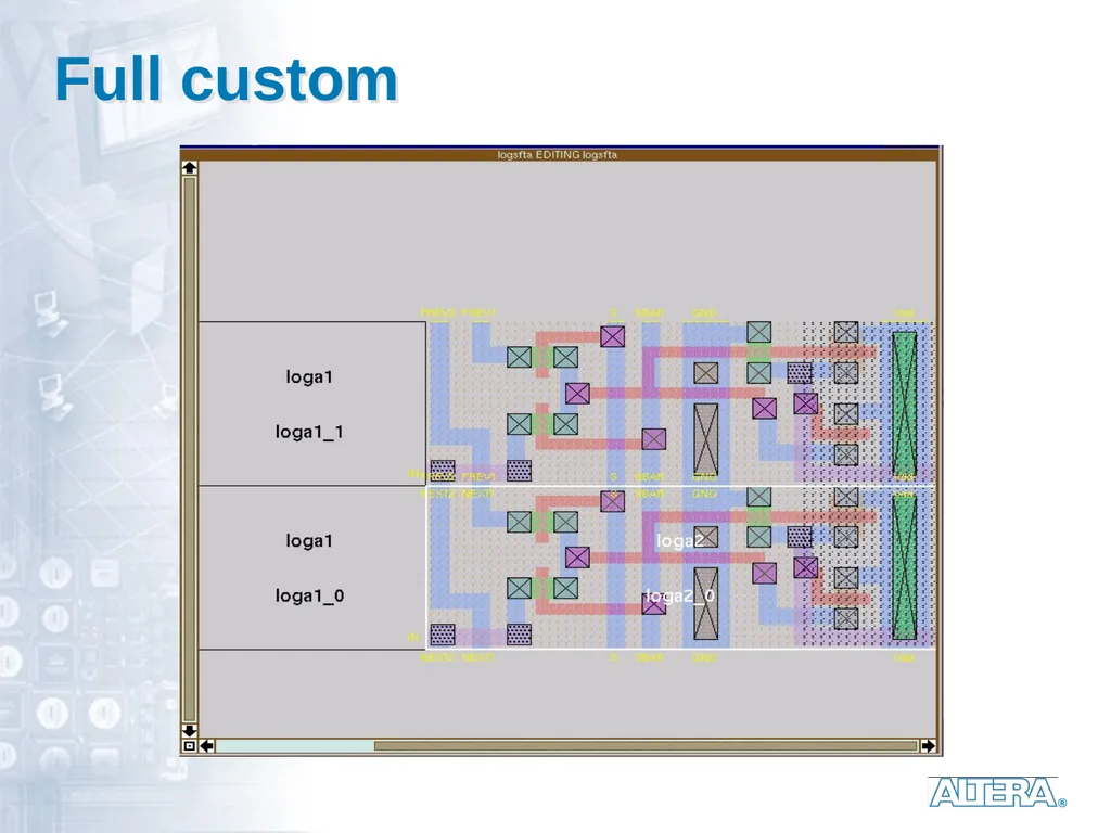
slide10. Full custom<br>
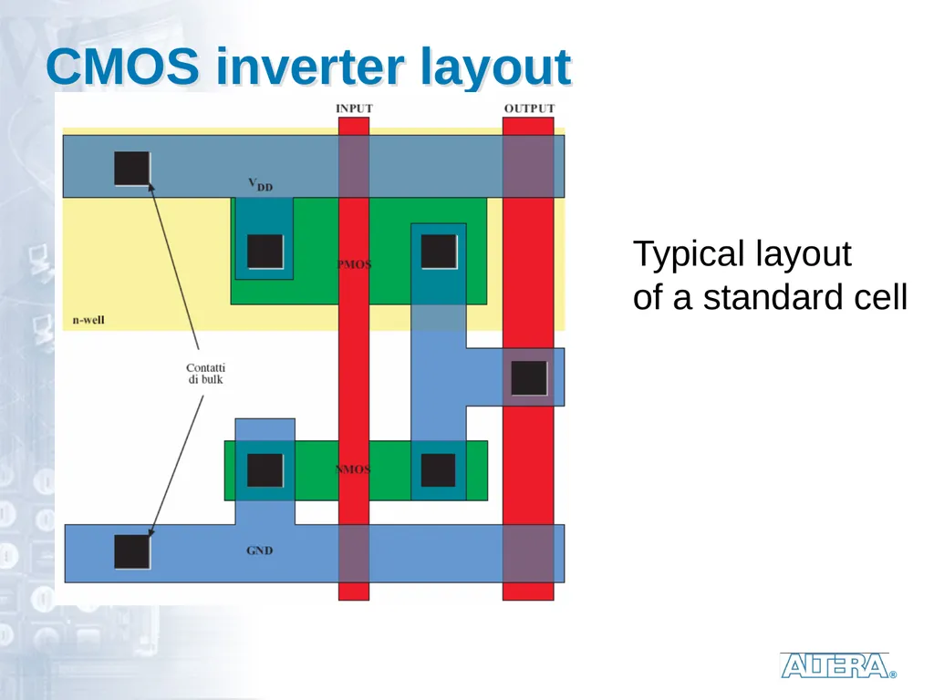
slide11. CMOS inverter layout Typical layout
of a standard cell<br>
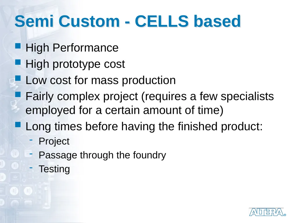
slide12. Semi Custom - CELLS based High Performance
High prototype cost
Low cost for mass production
Fairly complex project (requires a few specialists employed for a certain amount of time)
Long times before having the finished product:
Project
Passage through the foundry
Testing<br>
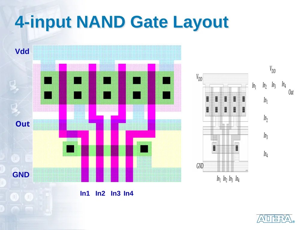
slide13. 4-input NAND Gate Layout In1 In2 In3 In4 Vdd GND Out<br>
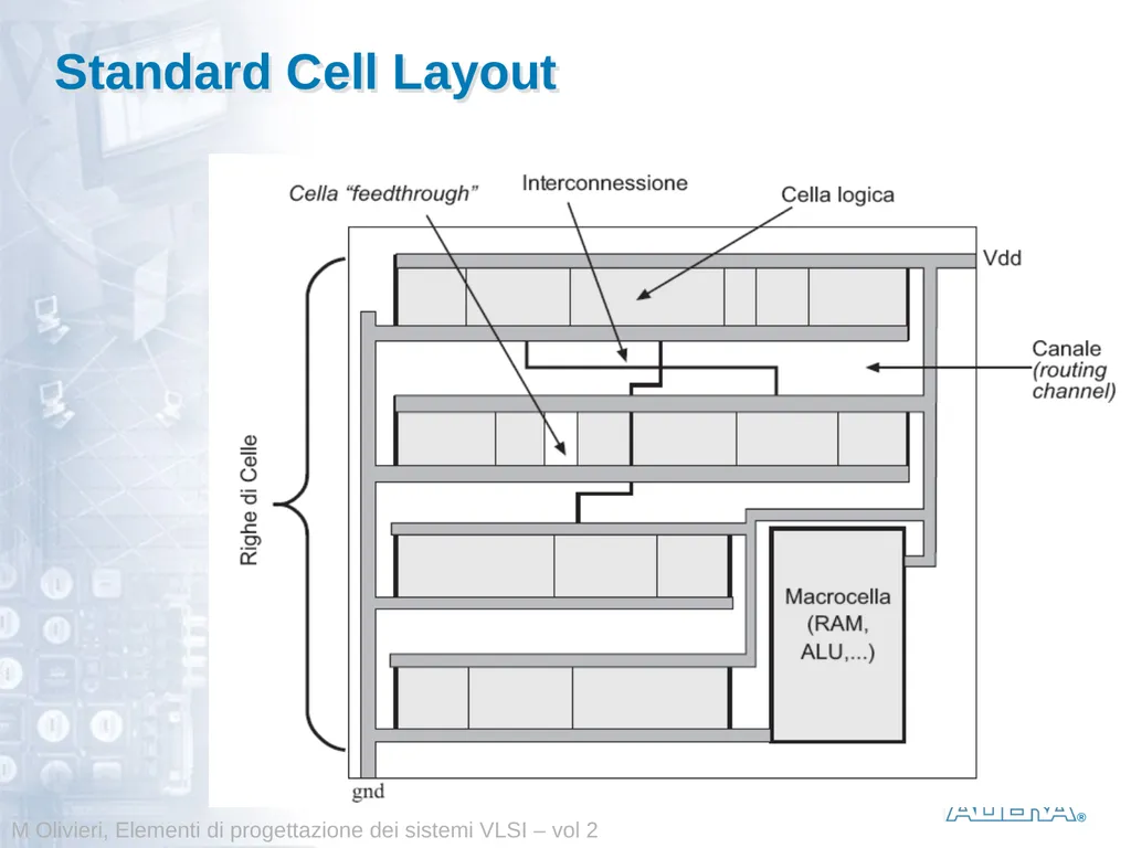
slide14. Standard Cell Layout M Olivieri, Elementi di progettazione dei sistemi VLSI – vol 2<br>
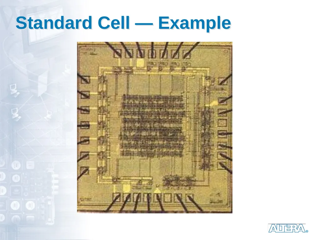
slide15. Standard Cell — Example<br>
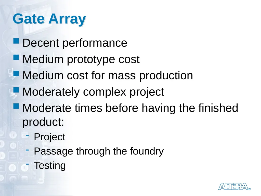
slide16. Gate Array Decent performance
Medium prototype cost
Medium cost for mass production
Moderately complex project
Moderate times before having the finished product:
Project
Passage through the foundry
Testing<br>
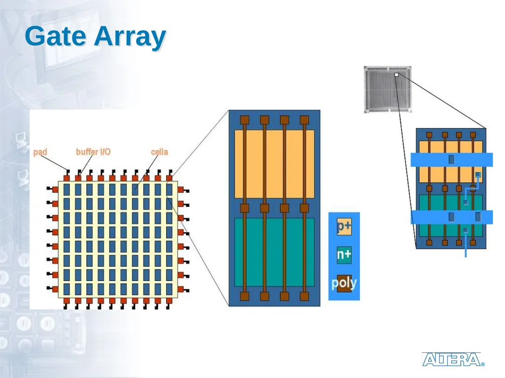
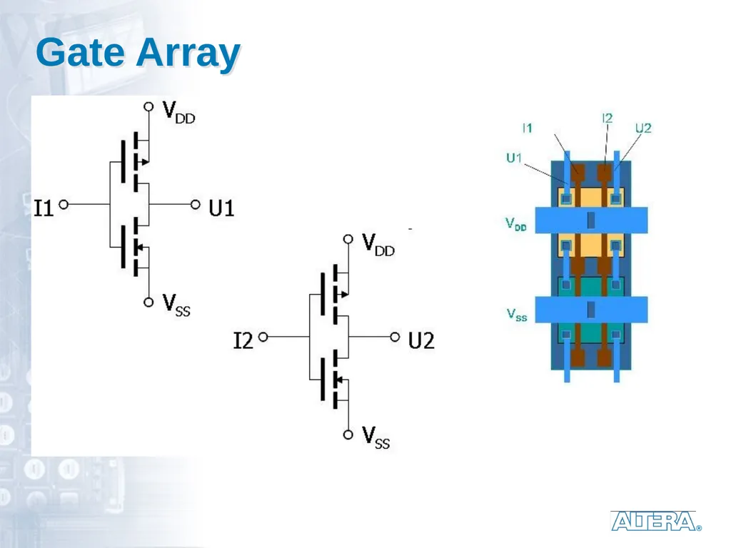
slide17. Gate Array<br>
slide18. Gate Array<br>
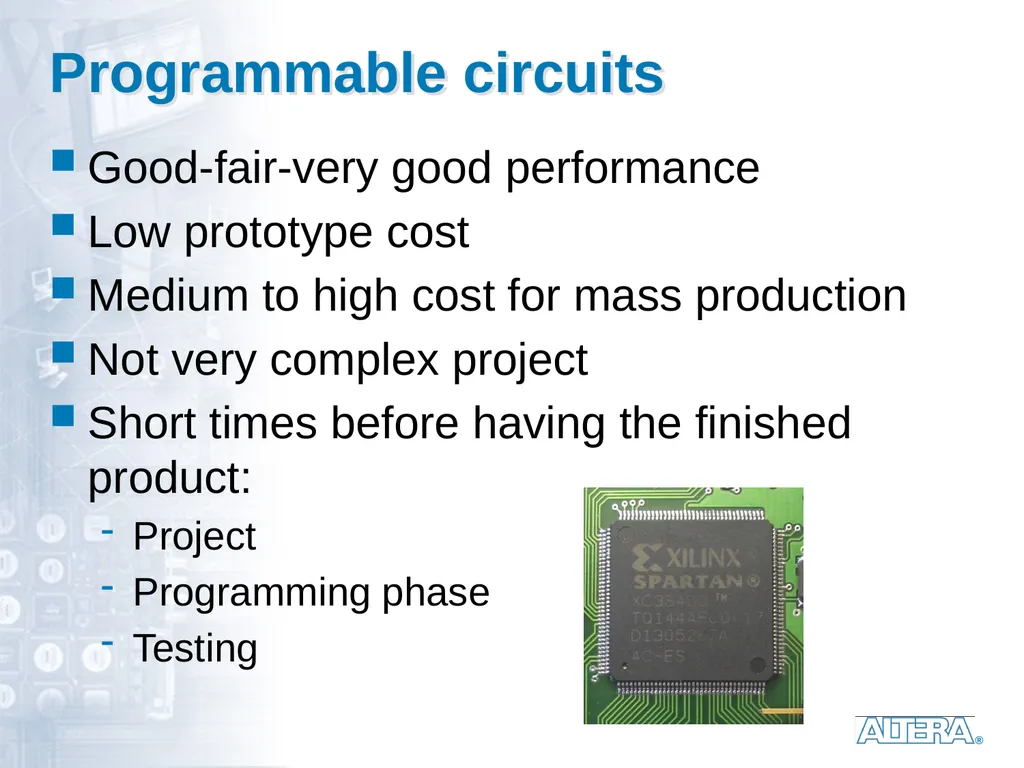
slide19. Programmable circuits Good-fair-very good performance
Low prototype cost
Medium to high cost for mass production
Not very complex project
Short times before having the finished product:
Project
Programming phase
Testing<br>
slide20. Conclusions The gap between programmable devices and ASICs is closing thanks to
Introduction of very low cost FPGAs.
Introduction of high-performance FPGAs.
Possible possibility of making an FPGA configurable through masks in the foundry
The market and production of FPGAs is constantly growing.<br>

slide2. Electronic Components Source: Dataquest Programmable
Logic Devices
(PLDs) Gate
Arrays Cell-Based
ICs Full Custom
ICs SPLDs
(PALs) FPGAs Acronyms
ASIC = Application Specific IC
SPLD = Simple Prog. Logic Device
PAL = Prog. Array of Logic
CPLD = Complex PLD
FPGA = Field Prog. Gate Array Common Resources
Configurable Logic Blocks (CLB)
Memory Look-Up Table
AND-OR planes
Simple gates
Input / Output Blocks (IOB)
Bidirectional, latches, inverters, pullup/pulldowns
Interconnect or Routing
Local, internal feedback, and global<br>
slide3. Key parameters Number of pieces to be produced
Cost of the prototype
Cost of the chip in production
Performance:
Occupied area
Working frequency
Power dissipation
Time to Market<br>
slide4. Glue logic By now unfeasible for any circuit that is not purely didactic or extremely simple:
High cost
Poor performance
Very high area
Very high power dissipation<br>
slide5. Full Custom Great performance
Very high prototype cost
Low cost for mass production
Very complex and laborious project (requires a group of specialists occupied for some time)
Long times before having the finished product:
Project
Passage through the foundry
Testing<br>
slide6. MOS transistor<br>
slide7. Layout layers representation<br>
slide8. MOS transistor representation<br>
slide9. Design rules (layout rules)<br>
slide10. Full custom<br>
slide11. CMOS inverter layout Typical layout
of a standard cell<br>
slide12. Semi Custom - CELLS based High Performance
High prototype cost
Low cost for mass production
Fairly complex project (requires a few specialists employed for a certain amount of time)
Long times before having the finished product:
Project
Passage through the foundry
Testing<br>
slide13. 4-input NAND Gate Layout In1 In2 In3 In4 Vdd GND Out<br>
slide14. Standard Cell Layout M Olivieri, Elementi di progettazione dei sistemi VLSI – vol 2<br>
slide15. Standard Cell — Example<br>
slide16. Gate Array Decent performance
Medium prototype cost
Medium cost for mass production
Moderately complex project
Moderate times before having the finished product:
Project
Passage through the foundry
Testing<br>
slide17. Gate Array<br>
slide18. Gate Array<br>
slide19. Programmable circuits Good-fair-very good performance
Low prototype cost
Medium to high cost for mass production
Not very complex project
Short times before having the finished product:
Project
Programming phase
Testing<br>
slide20. Conclusions The gap between programmable devices and ASICs is closing thanks to
Introduction of very low cost FPGAs.
Introduction of high-performance FPGAs.
Possible possibility of making an FPGA configurable through masks in the foundry
The market and production of FPGAs is constantly growing.<br>