
Digital Logic Design Lecture 24 Announcements


Description: Digital Logic Design Lecture 24 Announcements Homework 8 due today Exam 3 on Tuesday, 1125. Topics for exam are up on the course webpage. Agenda Last time: Master-Slave Flip-Flops (6.4) Edge-Triggered Flip-Flops (6.5) Characteristic
Related Topics
Download Presentation
"Digital Logic Design Lecture 24 Announcements" is the property of its rightful owner. Permission is granted to download and print the materials on this website for personal, non-commercial use only, and to display it on your personal computer provided you do not modify the materials and that you retain all copyright notices contained in the materials. By downloading content from our website, you accept the terms of this agreement.
Presentation Transcript
slide1. Digital Logic Design Lecture 24<br>
slide2. Announcements Homework 8 due today
Exam 3 on Tuesday, 11/25.
Topics for exam are up on the course webpage.<br>
slide3. Agenda Last time:
Master-Slave Flip-Flops (6.4)
Edge-Triggered Flip-Flops (6.5)
Characteristic Equations (6.6)
This time:
Registers (6.7)
Counters (6.8-6.9)
Review<br>
slide4. Registers A collection of flip-flops taken as an entity.
Function: Hold information within a digital system so that it is available to the logic elements during the computing process.
Each combination of stored information is known as the state or content of the register.
Shift register: Registers that are capable of moving information upon the occurrence of a clock-signal.
Unidirectional
bidirectional<br>
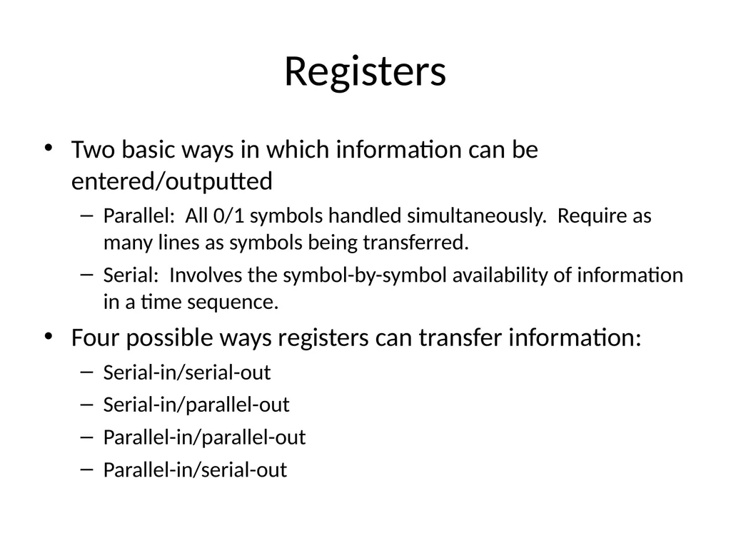
slide5. Registers Two basic ways in which information can be entered/outputted
Parallel: All 0/1 symbols handled simultaneously. Require as many lines as symbols being transferred.
Serial: Involves the symbol-by-symbol availability of information in a time sequence.
Four possible ways registers can transfer information:
Serial-in/serial-out
Serial-in/parallel-out
Parallel-in/parallel-out
Parallel-in/serial-out<br>
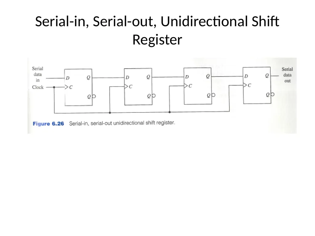
slide6. Serial-in, Serial-out, Unidirectional Shift Register<br>
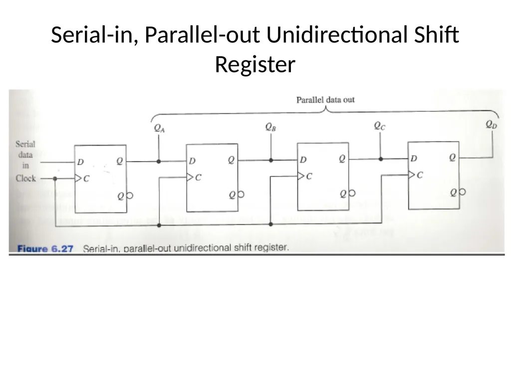
slide7. Serial-in, Parallel-out Unidirectional Shift Register<br>
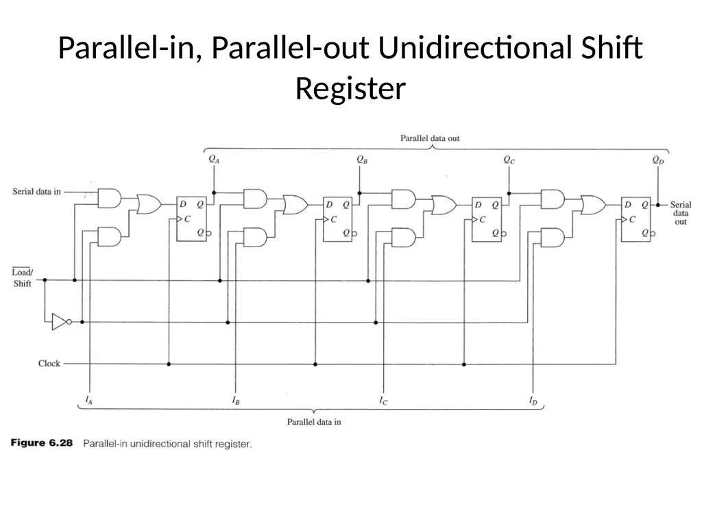
slide8. Parallel-in, Parallel-out Unidirectional Shift Register<br>
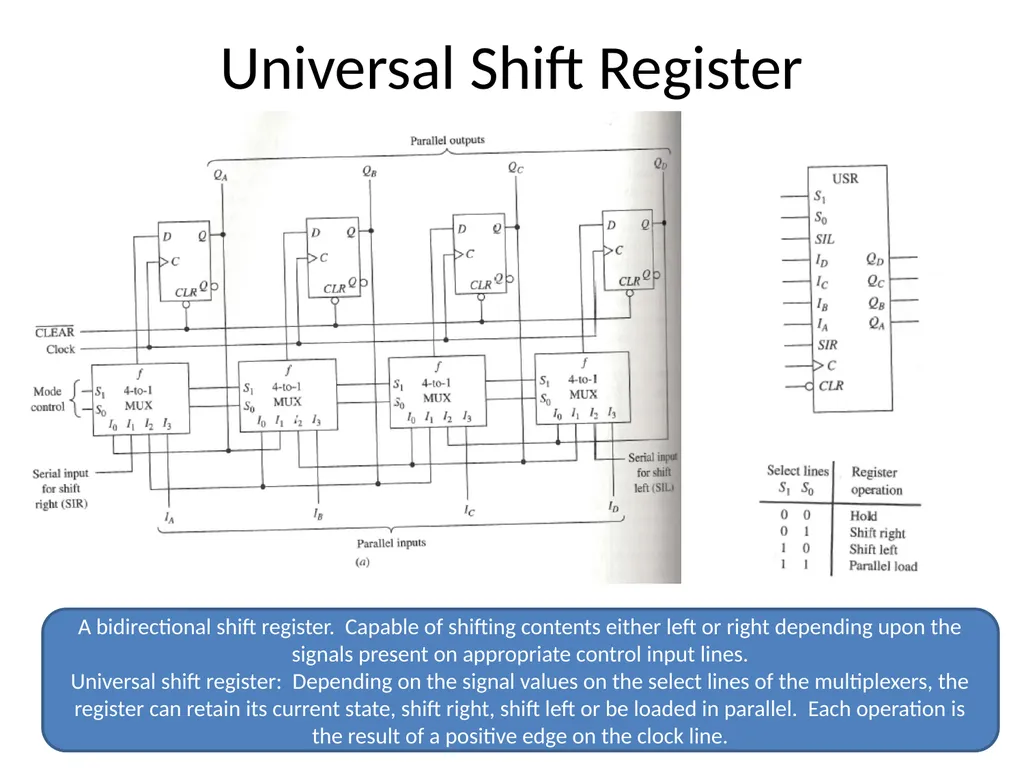
slide9. Universal Shift Register A bidirectional shift register. Capable of shifting contents either left or right depending upon the signals present on appropriate control input lines.
Universal shift register: Depending on the signal values on the select lines of the multiplexers, the register can retain its current state, shift right, shift left or be loaded in parallel. Each operation is the result of a positive edge on the clock line.<br>
slide10. Counters An example of a register.
Primary purpose is to produce a specified output pattern sequence.
Also called a pattern generator
Each stored 0/1 combination is called the state of the counter.
The total number of states is called its modulus.
If a counter has m distinct states then it is called a mod-m counter.
The order in which states appear is referred to as its counting sequence.
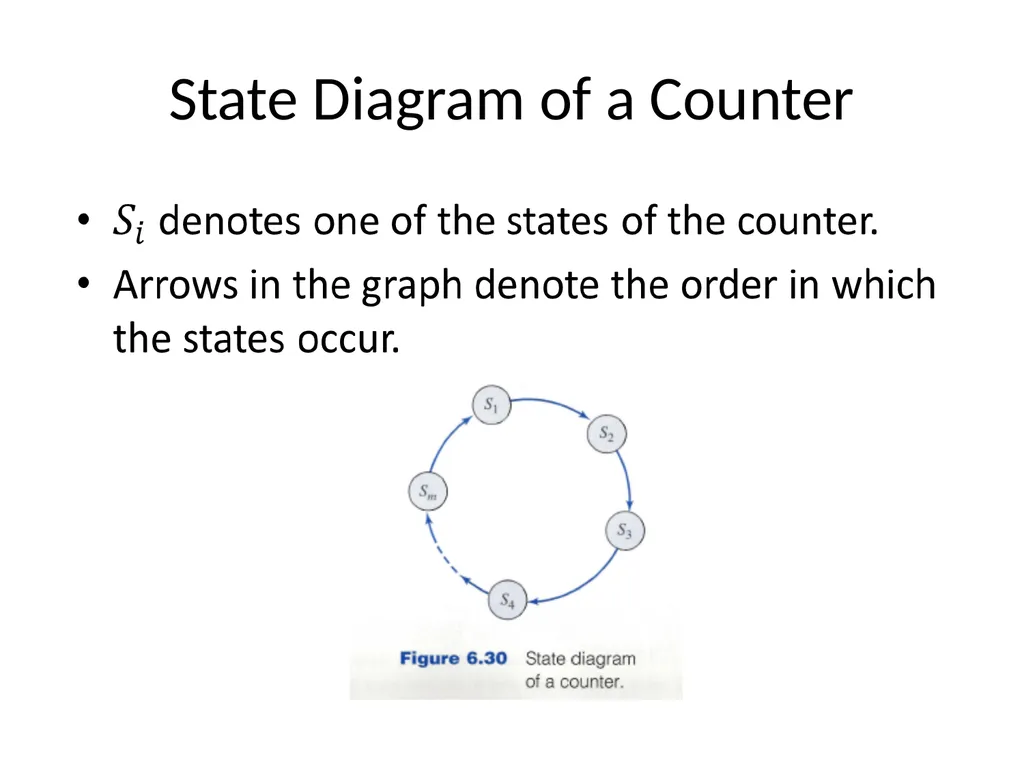
Depicted by a directed graph called a state diagram.<br>
slide11. State Diagram of a Counter<br>
slide12. Binary Ripple Counters<br>
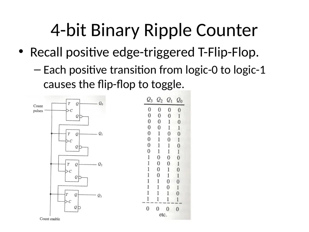
slide13. 4-bit Binary Ripple Counter Recall positive edge-triggered T-Flip-Flop.
Each positive transition from logic-0 to logic-1 causes the flip-flop to toggle.<br>
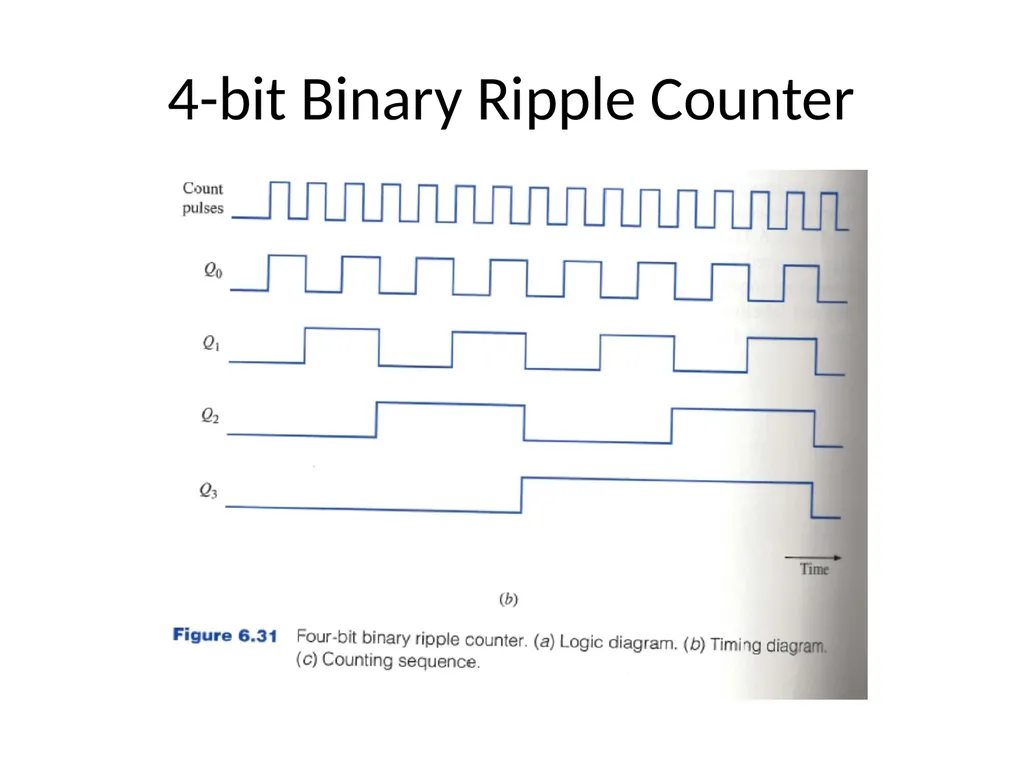
slide14. 4-bit Binary Ripple Counter<br>
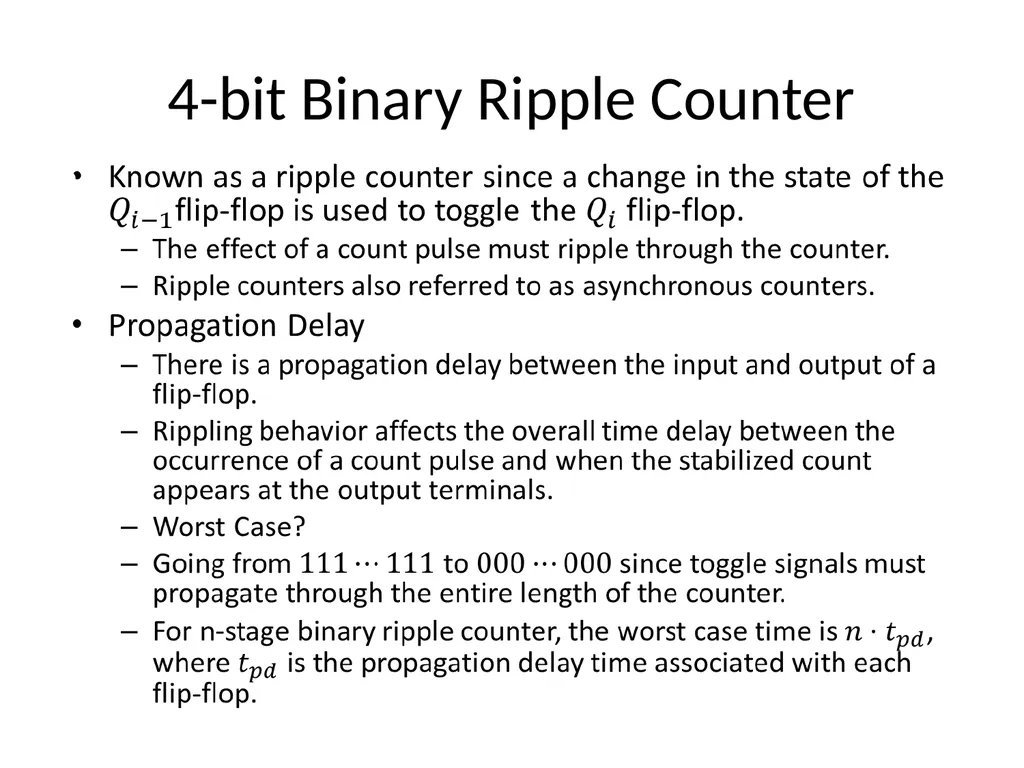
slide15. 4-bit Binary Ripple Counter<br>
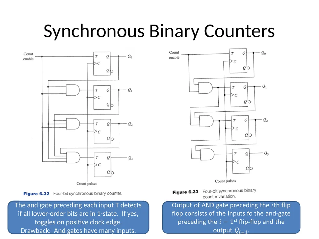
slide16. Synchronous Binary Counters All flip-flops change simultaneously after the appropriate propagation delay associated with a single flip-flop.
Count pulses are applied directly to the control inputs, C, of all the clocked flip-flops.
All flip-flops change simultaneously after the appropriate propagation delay associated with a single flip-flop.<br>
slide17. Synchronous Binary Counters The and gate preceding each input T detects if all lower-order bits are in 1-state. If yes, toggles on positive clock edge.
Drawback: And gates have many inputs.<br>
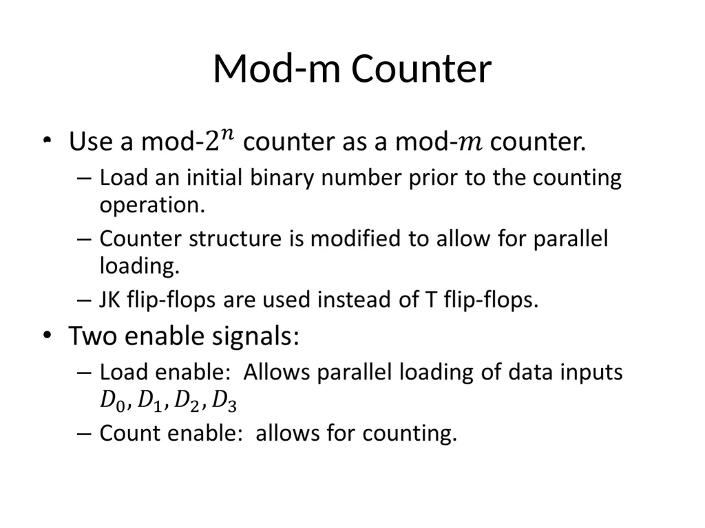
slide18. Mod-m Counter<br>
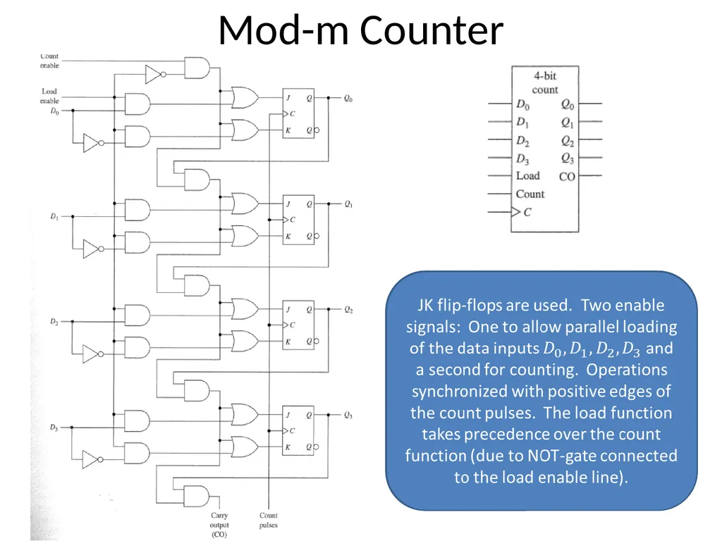
slide19. Mod-m Counter<br>
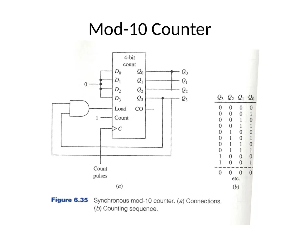
slide20. Mod-10 Counter<br>
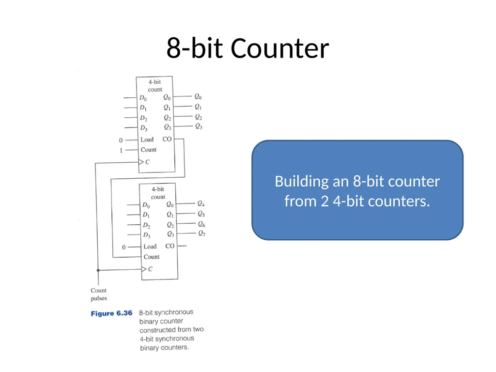
slide21. 8-bit Counter Building an 8-bit counter from 2 4-bit counters.<br>
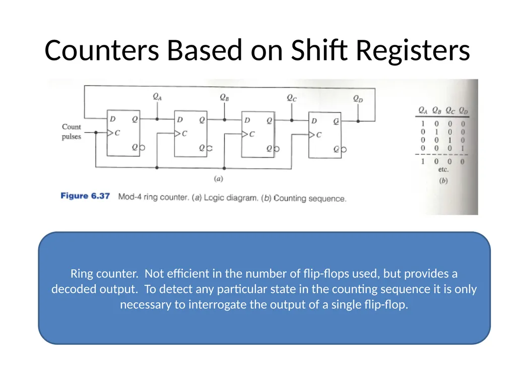
slide22. Counters Based on Shift Registers Ring counter. Not efficient in the number of flip-flops used, but provides a decoded output. To detect any particular state in the counting sequence it is only necessary to interrogate the output of a single flip-flop.<br>
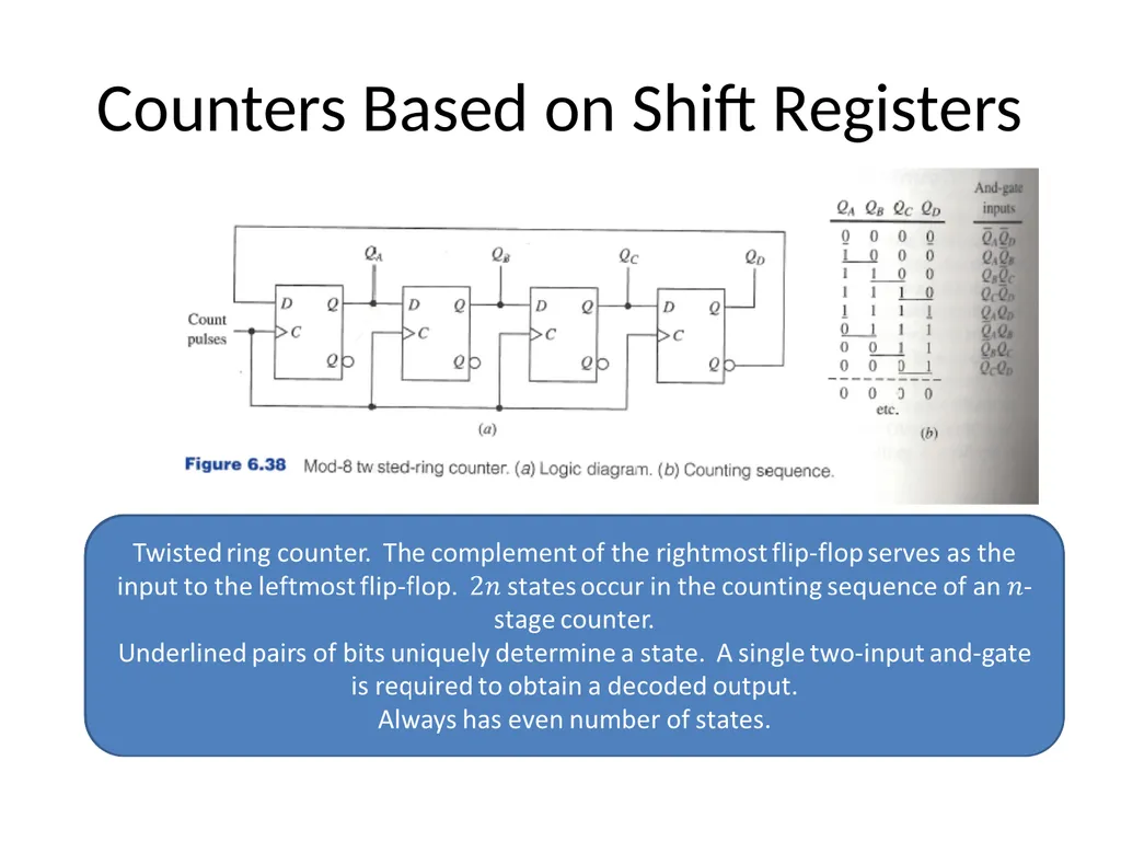
slide23. Counters Based on Shift Registers<br>
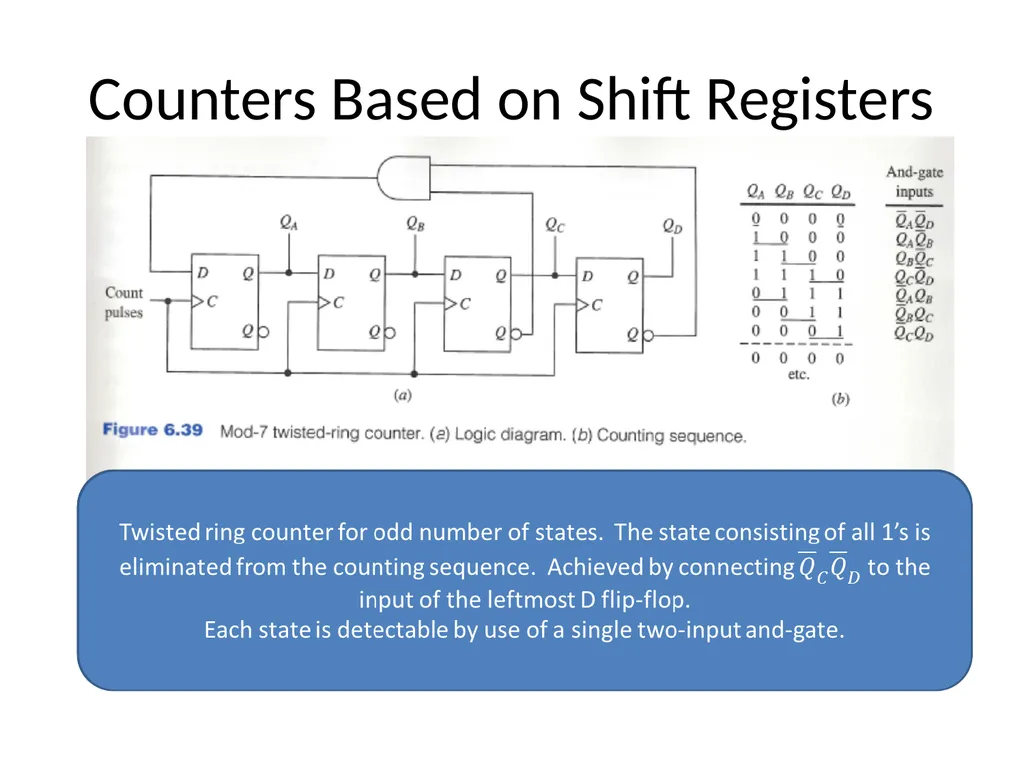
slide24. Counters Based on Shift Registers<br>
slide2. Announcements Homework 8 due today
Exam 3 on Tuesday, 11/25.
Topics for exam are up on the course webpage.<br>
slide3. Agenda Last time:
Master-Slave Flip-Flops (6.4)
Edge-Triggered Flip-Flops (6.5)
Characteristic Equations (6.6)
This time:
Registers (6.7)
Counters (6.8-6.9)
Review<br>
slide4. Registers A collection of flip-flops taken as an entity.
Function: Hold information within a digital system so that it is available to the logic elements during the computing process.
Each combination of stored information is known as the state or content of the register.
Shift register: Registers that are capable of moving information upon the occurrence of a clock-signal.
Unidirectional
bidirectional<br>
slide5. Registers Two basic ways in which information can be entered/outputted
Parallel: All 0/1 symbols handled simultaneously. Require as many lines as symbols being transferred.
Serial: Involves the symbol-by-symbol availability of information in a time sequence.
Four possible ways registers can transfer information:
Serial-in/serial-out
Serial-in/parallel-out
Parallel-in/parallel-out
Parallel-in/serial-out<br>
slide6. Serial-in, Serial-out, Unidirectional Shift Register<br>
slide7. Serial-in, Parallel-out Unidirectional Shift Register<br>
slide8. Parallel-in, Parallel-out Unidirectional Shift Register<br>
slide9. Universal Shift Register A bidirectional shift register. Capable of shifting contents either left or right depending upon the signals present on appropriate control input lines.
Universal shift register: Depending on the signal values on the select lines of the multiplexers, the register can retain its current state, shift right, shift left or be loaded in parallel. Each operation is the result of a positive edge on the clock line.<br>
slide10. Counters An example of a register.
Primary purpose is to produce a specified output pattern sequence.
Also called a pattern generator
Each stored 0/1 combination is called the state of the counter.
The total number of states is called its modulus.
If a counter has m distinct states then it is called a mod-m counter.
The order in which states appear is referred to as its counting sequence.
Depicted by a directed graph called a state diagram.<br>
slide11. State Diagram of a Counter<br>
slide12. Binary Ripple Counters<br>
slide13. 4-bit Binary Ripple Counter Recall positive edge-triggered T-Flip-Flop.
Each positive transition from logic-0 to logic-1 causes the flip-flop to toggle.<br>
slide14. 4-bit Binary Ripple Counter<br>
slide15. 4-bit Binary Ripple Counter<br>
slide16. Synchronous Binary Counters All flip-flops change simultaneously after the appropriate propagation delay associated with a single flip-flop.
Count pulses are applied directly to the control inputs, C, of all the clocked flip-flops.
All flip-flops change simultaneously after the appropriate propagation delay associated with a single flip-flop.<br>
slide17. Synchronous Binary Counters The and gate preceding each input T detects if all lower-order bits are in 1-state. If yes, toggles on positive clock edge.
Drawback: And gates have many inputs.<br>
slide18. Mod-m Counter<br>
slide19. Mod-m Counter<br>
slide20. Mod-10 Counter<br>
slide21. 8-bit Counter Building an 8-bit counter from 2 4-bit counters.<br>
slide22. Counters Based on Shift Registers Ring counter. Not efficient in the number of flip-flops used, but provides a decoded output. To detect any particular state in the counting sequence it is only necessary to interrogate the output of a single flip-flop.<br>
slide23. Counters Based on Shift Registers<br>
slide24. Counters Based on Shift Registers<br>