Electron-beam lithography with the Raith EBPG Part 4: Alignment Marks M. Rooks, Yale University Alignment Marks Alignment marks, or markers are used to align one layer of lithography with another layer. For example, if you need to print
"Electron-beam lithography with the Raith EBPG Part" is the property of its rightful owner. Permission is granted to
download and print the materials on this website for personal, non-commercial use only, and to display it
on your personal computer provided you do not modify the materials and that you retain all copyright
notices contained in the materials. By downloading content from our website, you accept the terms of this
agreement.
Presentation Transcript
01
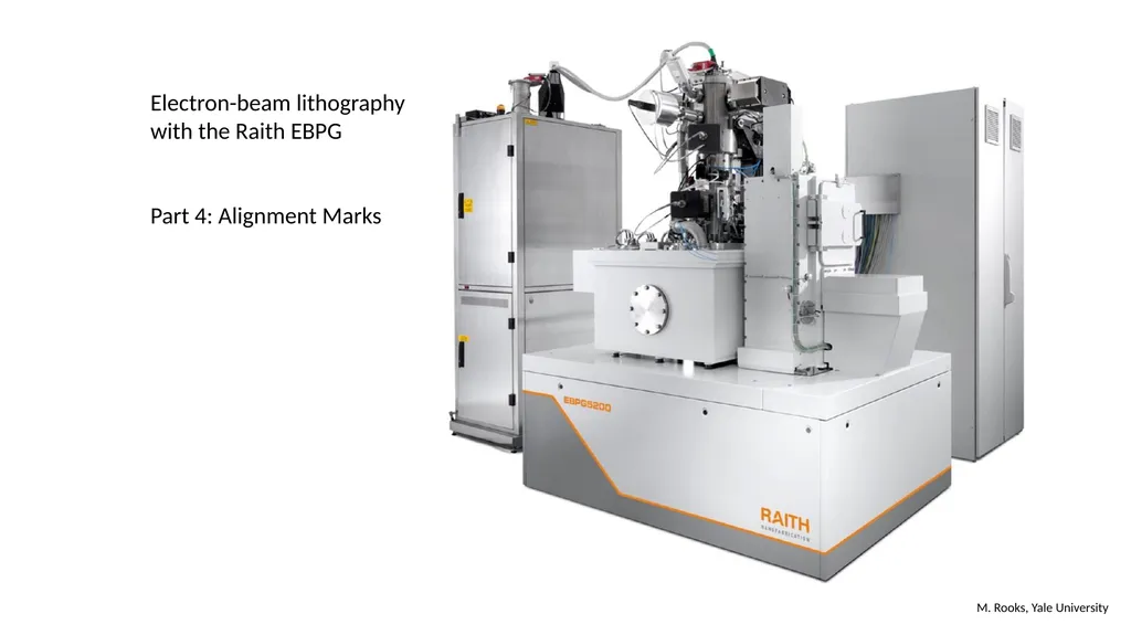
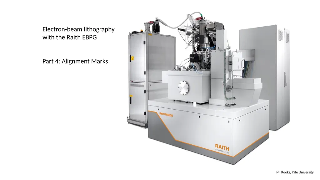
Electron-beam lithography with the Raith EBPG
Part 4: Alignment Marks M. Rooks, Yale University<br>
02
Alignment Marks
Alignment marks, or “markers” are used to align one layer of lithography with another layer. For example, if you need to print small, thin wires that connect to large, thick pads, then you will need alignment marks so that you can use two separate liftoff steps.
Alignment marks for the EBPG are usually squares, but they can also be rectangles or crosses. There are other crazy shapes you might use, but you should not.
Alignment marks range in size from ~4mm to 100mm on a side.<br>
03
chip Alignment strategy
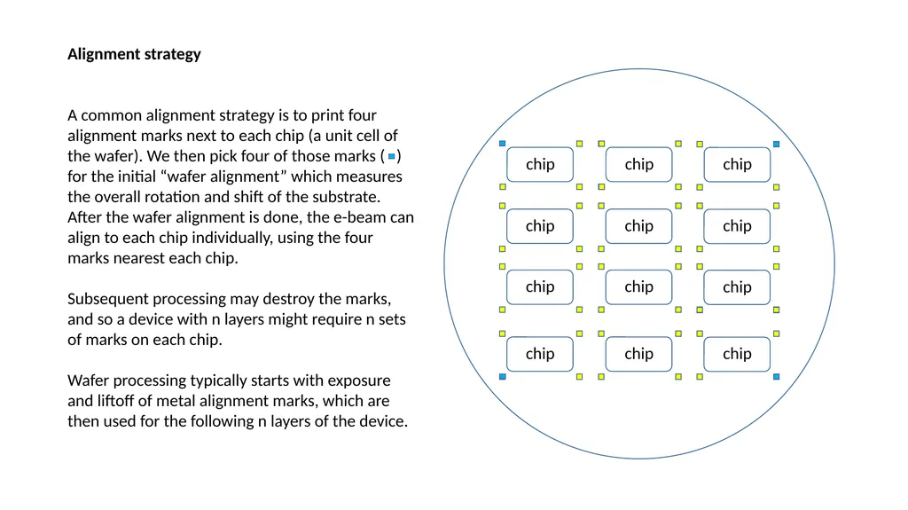
A common alignment strategy is to print four alignment marks next to each chip (a unit cell of the wafer). We then pick four of those marks ( ) for the initial “wafer alignment” which measures the overall rotation and shift of the substrate. After the wafer alignment is done, the e-beam can align to each chip individually, using the four marks nearest each chip.
Subsequent processing may destroy the marks, and so a device with n layers might require n sets of marks on each chip.
Wafer processing typically starts with exposure and liftoff of metal alignment marks, which are then used for the following n layers of the device.<br>
04
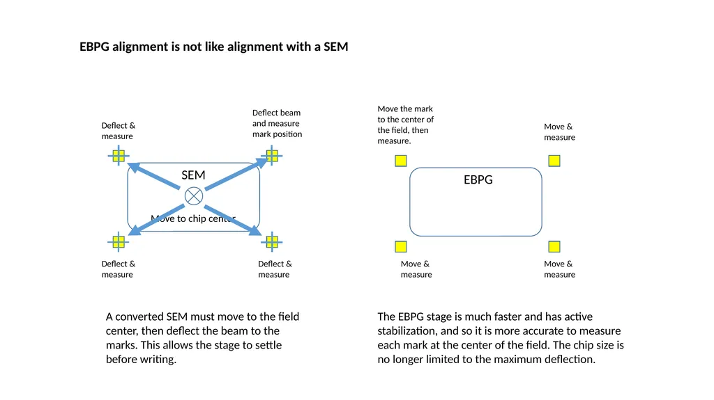
Move to chip center Deflect beam and measure mark position Deflect & measure Deflect & measure Deflect & measure Move the mark to the center of the field, then measure. Move & measure Move & measure Move & measure EBPG alignment is not like alignment with a SEM A converted SEM must move to the field center, then deflect the beam to the marks. This allows the stage to settle before writing. The EBPG stage is much faster and has active stabilization, and so it is more accurate to measure each mark at the center of the field. The chip size is no longer limited to the maximum deflection. SEM EBPG<br>
05
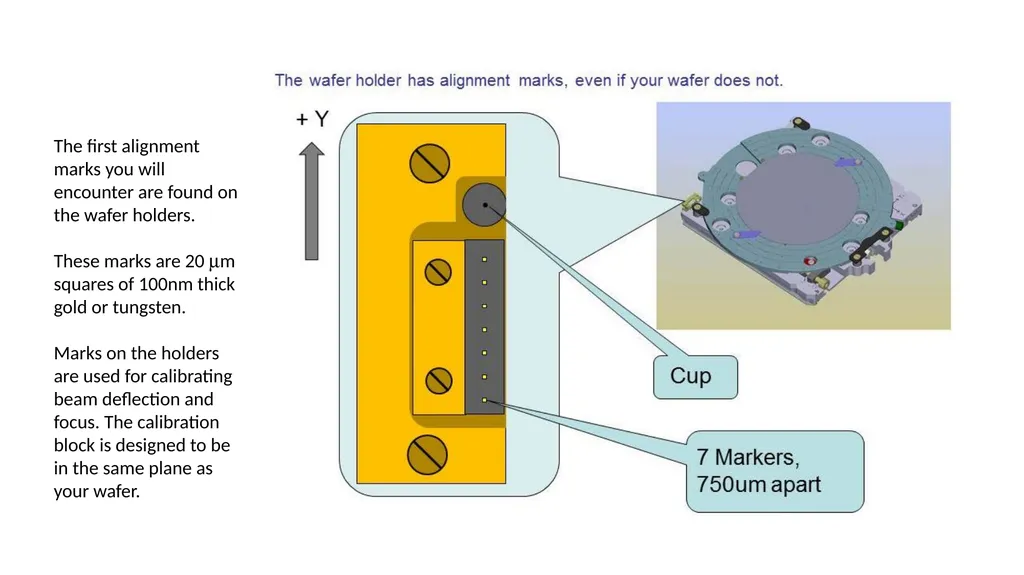
The first alignment marks you will encounter are found on the wafer holders.
These marks are 20 mm squares of 100nm thick gold or tungsten.
Marks on the holders are used for calibrating beam deflection and focus. The calibration block is designed to be in the same plane as your wafer.<br>
06
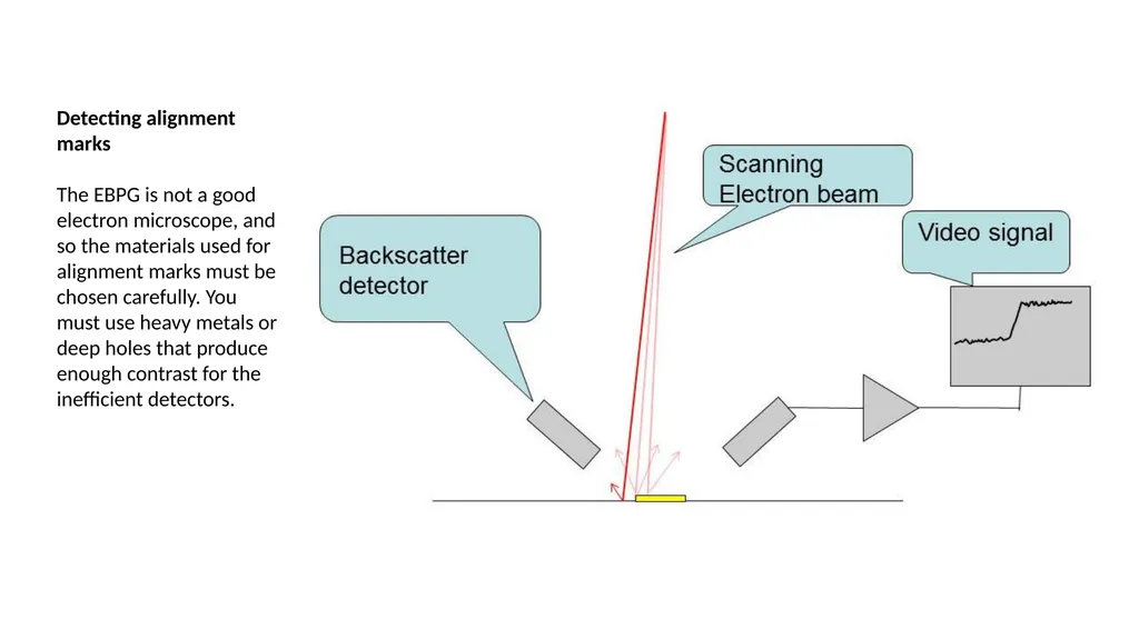
Detecting alignment marks
The EBPG is not a good electron microscope, and so the materials used for alignment marks must be chosen carefully. You must use heavy metals or deep holes that produce enough contrast for the inefficient detectors.<br>
07
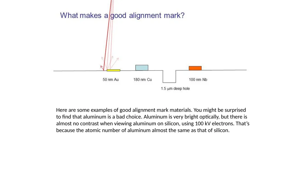
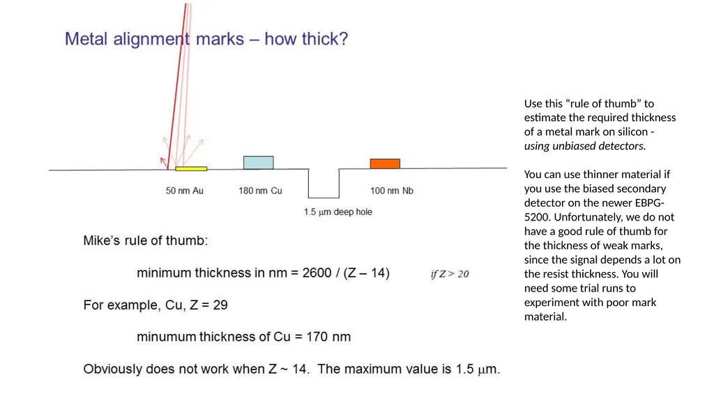
Here are some examples of good alignment mark materials. You might be surprised to find that aluminum is a bad choice. Aluminum is very bright optically, but there is almost no contrast when viewing aluminum on silicon, using 100 kV electrons. That’s because the atomic number of aluminum almost the same as that of silicon.<br>
08
Use this “rule of thumb” to estimate the required thickness of a metal mark on silicon - using unbiased detectors.
You can use thinner material if you use the biased secondary detector on the newer EBPG-5200. Unfortunately, we do not have a good rule of thumb for the thickness of weak marks, since the signal depends a lot on the resist thickness. You will need some trial runs to experiment with poor mark material.<br>
09
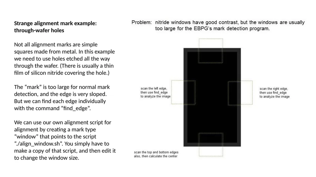
Strange alignment mark example: through-wafer holes
Not all alignment marks are simple squares made from metal. In this example we need to use holes etched all the way through the wafer. (There is usually a thin film of silicon nitride covering the hole.)
The “mark” is too large for normal mark detection, and the edge is very sloped. But we can find each edge individually with the command “find_edge”.
We can use our own alignment script for alignment by creating a mark type “window” that points to the script “./align_window.sh”. You simply have to make a copy of that script, and then edit it to change the window size.<br>
10
More strange alignment marks
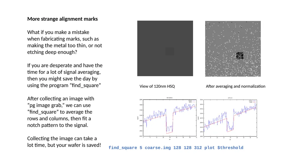
What if you make a mistake when fabricating marks, such as making the metal too thin, or not etching deep enough?
If you are desperate and have the time for a lot of signal averaging, then you might save the day by using the program “find_square”
After collecting an image with “pg image grab,” we can use “find_square” to average the rows and columns, then fit a notch pattern to the signal.
Collecting the image can take a lot time, but your wafer is saved! View of 120nm HSQ After averaging and normalization<br>
11
The strangest alignment marks: none at all
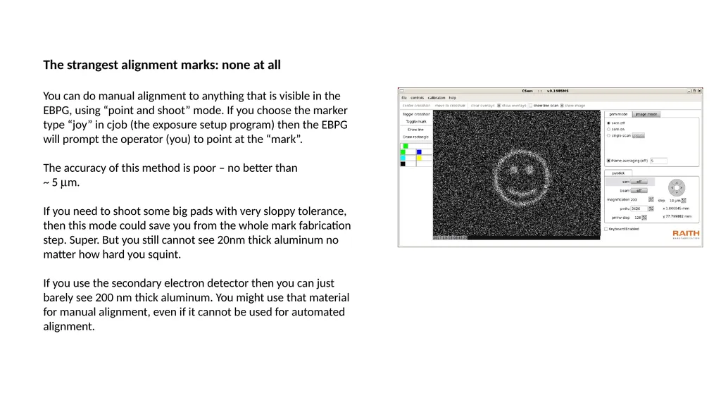
You can do manual alignment to anything that is visible in the EBPG, using “point and shoot” mode. If you choose the marker type “joy” in cjob (the exposure setup program) then the EBPG will prompt the operator (you) to point at the “mark”.
The accuracy of this method is poor – no better than ~ 5 mm.
If you need to shoot some big pads with very sloppy tolerance, then this mode could save you from the whole mark fabrication step. Super. But you still cannot see 20nm thick aluminum no matter how hard you squint.
If you use the secondary electron detector then you can just barely see 200 nm thick aluminum. You might use that material for manual alignment, even if it cannot be used for automated alignment.<br>
12
Common mistakes with alignment
Before you spend a lot of time with CAD and before you print mask plates, have an experienced person idiot-check your design. They might find some of these common errors:
Marks are too thin or too shallow
Processing destroys the marks
The marks are too small to see in an optical microscope
Your substrate is too small, and so pre-alignment will be difficult
Marks are near the edge of the substrate, where the height sensor cannot reach
You think there must be alignment marks in every field<br>