
Flip - Flops Qusay H Ali Digital logic design 4th



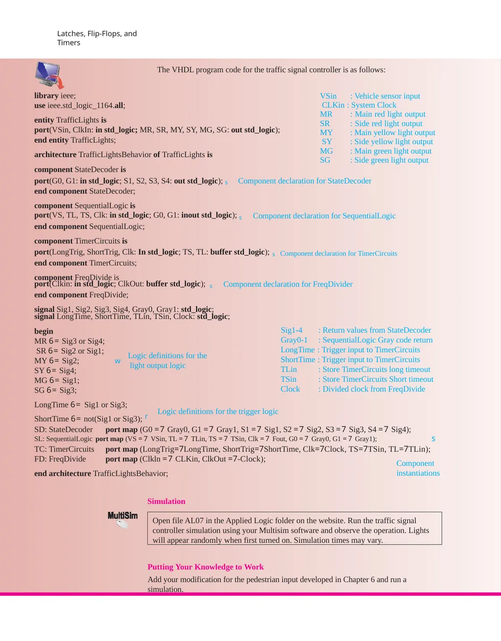
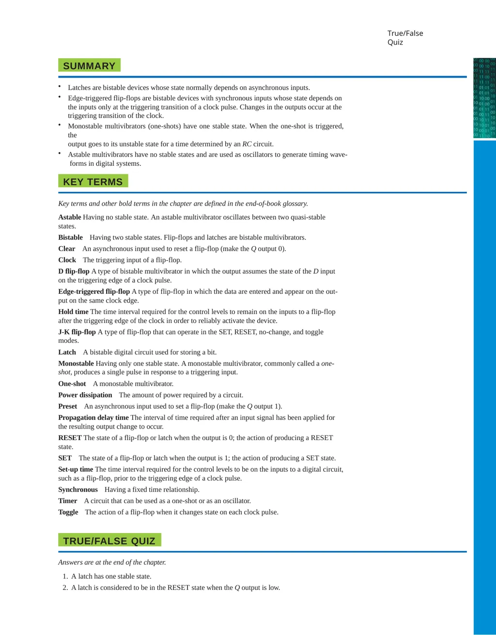
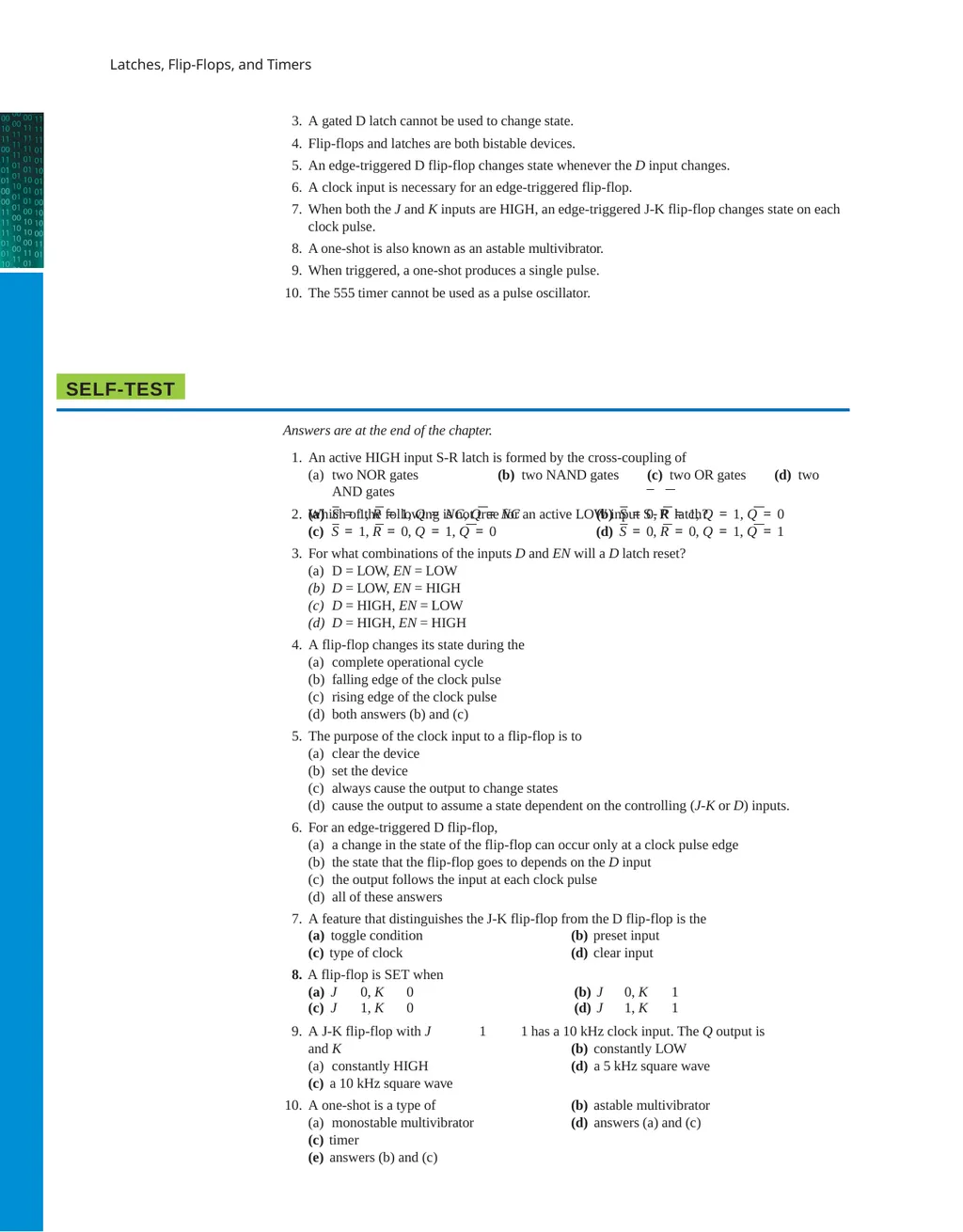
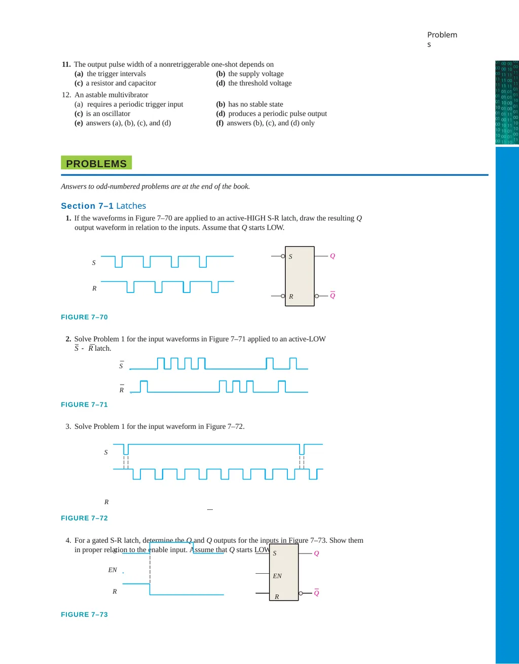
Description: Flip - Flops Qusay H Ali Digital logic design 4th semester Week no. 387 CHAPTER OUTLINE 71 Latches 72 Flip-Flops 73 Flip-Flop Operating Characteristics 74 Flip-Flop Applications 75 One-Shots 76 The Astable Multivibrator 77
Related Topics
Download Presentation
"Flip - Flops Qusay H Ali Digital logic design 4th" is the property of its rightful owner. Permission is granted to download and print the materials on this website for personal, non-commercial use only, and to display it on your personal computer provided you do not modify the materials and that you retain all copyright notices contained in the materials. By downloading content from our website, you accept the terms of this agreement.
Presentation Transcript
slide1. Flip - Flops Qusay H Ali
Digital logic design
4th semester
Week no.<br>
slide2. 387 CHAPTER OUTLINE 7–1 Latches
7–2 Flip-Flops
7–3 Flip-Flop Operating Characteristics
7–4 Flip-Flop Applications
7–5 One-Shots
7–6 The Astable Multivibrator
7–7 Troubleshooting
Applied Logic CHAPTER OBJECTIVES
Use logic gates to construct basic latches
Explain the difference between an S-R latch and a D latch
Recognize the difference between a latch and a flip-flop
Explain how D and J-K flip-flops differ
Understand the significance of propagation delays, set-up time, hold time, maximum operating
frequency, minimum clock pulse widths, and power dissipation in the application of flip-flops
Apply flip-flops in basic applications
Explain how retriggerable and nonretriggerable one-shots differ
Connect a 555 timer to operate as either an astable multivibrator or a one-shot
Describe latches, flip-flops, and timers using VHDL
Troubleshoot basic flip-flop circuits VISIT THE WEBSITE
Study aids for this chapter are available at http://www.pearsonglobaleditions.com/floyd INTRODUCTION
This chapter begins a study of the fundamentals of sequential logic. Bistable, monostable, and astable logic devices called multivibrators are covered. Two categories of bistable devices are the latch and the flip-flop. Bistable devices have two stable states, called SET and RESET; they can retain either of these states indefinitely, making them useful as stor- age devices. The basic difference between latches and flip-flops is the way in which they are changed from one state to the other. The flip-flop is a basic building block for counters, registers, and other sequential control logic and is used in certain types of memories. The monostable multivibrator, commonly known as the one-shot, has only one stable state.
A one-shot produces a single controlled-width pulse when activated or triggered. The astable multivibrator has no stable state and is used primarily as an oscil- lator, which is a self-sustained waveform generator. Pulse oscillators are used as the sources for timing waveforms in digital systems. Clock
Edge-triggered flip-flop
D flip-flop
Synchronous
J-K flip-flop
Toggle
Preset
Clear Propagation delay time
Set-up time
Hold time
Power dissipation
One-shot
Monostable
Timer
Astable Latches, Flip-Flops, and Timers 7 CHAPTER Latch
Bistable SET
RESET KEY TERMS
Key terms are in order of appearance in the chapter.<br>
slide3. Latches, Flip-Flops, and Timers 7–1 Latches The latch is a type of temporary storage device that has two stable states (bistable) and is normally placed in a category separate from that of flip-flops. Latches are similar to flip-flops because they are bistable devices that can reside in either of two states using a feedback arrangement, in which the outputs are connected back to the opposite inputs. The main difference between latches and flip-flops is in the method used for changing their state.
After completing this section, you should be able to ◆ Explain the operation of a basic S-R latch Explain the operation of a gated S-R latch Explain the operation of a gated D latch Implement an S-R or D latch with logic gates
Describe the 74HC279A and 74HC75 quad latches ◆ ◆ ◆ ◆ The S-R (SET-RESET) Latch
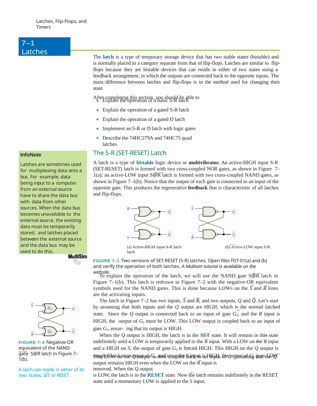
A latch is a type of bistable logic device or multivibrator. An active-HIGH input S-R (SET-RESET) latch is formed with two cross-coupled NOR gates, as shown in Figure 7–1(a); an active-LOW input S@R latch is formed with two cross-coupled NAND gates, as shown in Figure 7–1(b). Notice that the output of each gate is connected to an input of the opposite gate. This produces the regenerative feedback that is characteristic of all latches and flip-flops. InfoNote
Latches are sometimes used for multiplexing data onto a bus. For example, data being input to a computer from an external source have to share the data bus with data from other sources. When the data bus becomes unavailable to the external source, the existing data must be temporarily stored, and latches placed between the external source and the data bus may be used to do this. R S Q Q S R Q Q (a) Active-HIGH input S-R latch (b) Active-LOW input S-R latch
FIGURE 7–1 Two versions of SET-RESET (S-R) latches. Open files F07-01(a) and (b) and verify the operation of both latches. A Multisim tutorial is available on the website. To explain the operation of the latch, we will use the NAND gate S@R latch in Figure 7–1(b). This latch is redrawn in Figure 7–2 with the negative-OR equivalent symbols used for the NAND gates. This is done because LOWs on the S and R lines are the activating inputs.
The latch in Figure 7–2 has two inputs, S and R, and two outputs, Q and Q. Let’s start by assuming that both inputs and the Q output are HIGH, which is the normal latched state. Since the Q output is connected back to an input of gate G2, and the R input is HIGH, the output of G2 must be LOW. This LOW output is coupled back to an input of gate G1, ensur- ing that its output is HIGH.
When the Q output is HIGH, the latch is in the SET state. It will remain in this state indefinitely until a LOW is temporarily applied to the R input. With a LOW on the R input and a HIGH on S, the output of gate G2 is forced HIGH. This HIGH on the Q output is coupled back to an input of G1, and since the S input is HIGH, the output of G1 goes LOW. This LOW on the Q output is then coupled back to an input of G , ensuring that the Q 2
output remains HIGH even when the LOW on the R input is removed. When the Q output
is LOW, the latch is in the RESET state. Now the latch remains indefinitely in the RESET state until a momentary LOW is applied to the S input. Q Q S R G 1 G2 FIGURE 7–2 Negative-OR equivalent of the NAND gate S@R latch in Figure 7–1(b). A latch can reside in either of its two states, SET or RESET.<br>
slide4. Latches In normal operation, the outputs of a latch are always complements of each other.
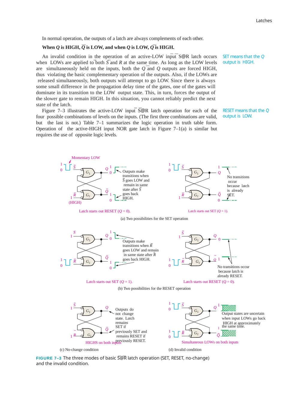
When Q is HIGH, Q is LOW, and when Q is LOW, Q is HIGH. An invalid condition in the operation of an active-LOW input S@R latch occurs when LOWs are applied to both S and R at the same time. As long as the LOW levels are simultaneously held on the inputs, both the Q and Q outputs are forced HIGH, thus violating the basic complementary operation of the outputs. Also, if the LOWs are released simultaneously, both outputs will attempt to go LOW. Since there is always some small difference in the propagation delay time of the gates, one of the gates will dominate in its transition to the LOW output state. This, in turn, forces the output of the slower gate to remain HIGH. In this situation, you cannot reliably predict the next state of the latch.
Figure 7–3 illustrates the active-LOW input S@R latch operation for each of the four possible combinations of levels on the inputs. (The first three combinations are valid, but the last is not.) Table 7–1 summarizes the logic operation in truth table form. Operation of the active-HIGH input NOR gate latch in Figure 7–1(a) is similar but requires the use of opposite logic levels. SET means that the Q output is HIGH. RESET means that the Q output is LOW. Q Q S R G 1 G2 1
0 1
0 1 Output states are uncertain when input LOWs go back HIGH at approximately
1 the same time. Simultaneous LOWs on both inputs
(d) Invalid condition (b) Two possibilities for the RESET operation Q Q S G 1 R G2 1 Outputs do not change state. Latch
remains SET if
previously SET and remains RESET if previously RESET. HIGHS on both inputs
(c) No-change condition 1 1
Q Q
0 S R 1
0 1 No transitions occur because latch is already SET. Q S R G2 1
0 1 1 Q
0 1
0 (HIGH) Momentary LOW Latch starts out RESET (Q = 0). Latch starts out SET (Q = 1).
(a) Two possibilities for the SET operation Outputs make transitions when S goes LOW and remain in same state after S
goes back HIGH. G 1 Q S G 1 R G2 1
0 1 0 Q 1 No transitions occur because latch is already RESET.
Latch starts out RESET (Q = 0). Q R G 1 G2 S
1 1
Q 1
0 0 1
0 Outputs make transitions when R goes LOW and remain in same state after R goes back HIGH. Latch starts out SET (Q = 1). G2 G 1 FIGURE 7–3 The three modes of basic S@R latch operation (SET, RESET, no-change) and the invalid condition.<br>
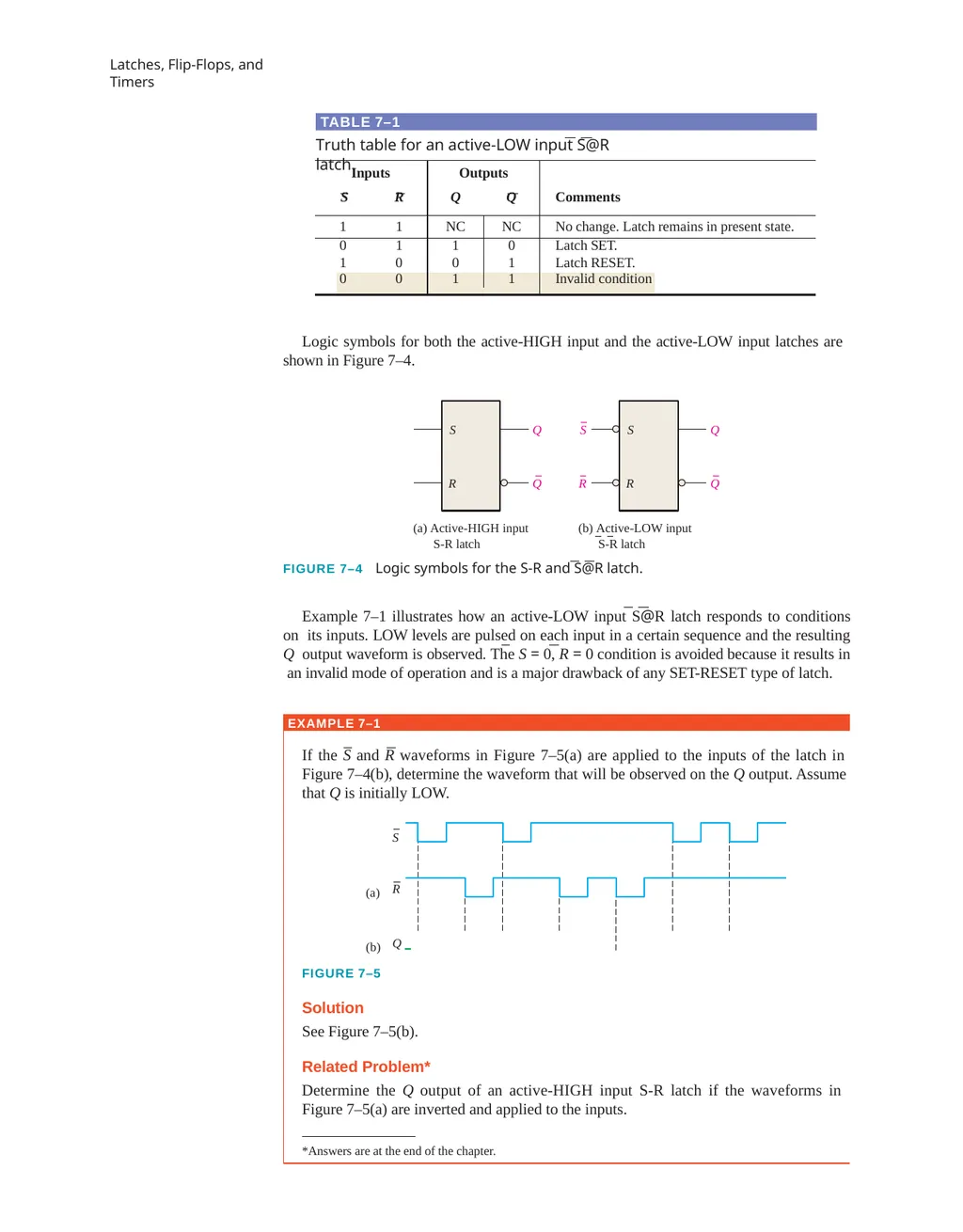
slide5. Latches, Flip-Flops, and Timers Logic symbols for both the active-HIGH input and the active-LOW input latches are shown in Figure 7–4. TABLE 7–1 Truth table for an active-LOW input S@R latch. Q Q S R S R Q Q S R (a) Active-HIGH input S-R latch (b) Active-LOW input S-R latch FIGURE 7–4 Logic symbols for the S-R and S@R latch.
Example 7–1 illustrates how an active-LOW input S@R latch responds to conditions on its inputs. LOW levels are pulsed on each input in a certain sequence and the resulting Q output waveform is observed. The S = 0, R = 0 condition is avoided because it results in an invalid mode of operation and is a major drawback of any SET-RESET type of latch. EXAMPLE 7–1 If the S and R waveforms in Figure 7–5(a) are applied to the inputs of the latch in Figure 7–4(b), determine the waveform that will be observed on the Q output. Assume that Q is initially LOW.
S (a) R Q (b) FIGURE 7–5
Solution
See Figure 7–5(b).
Related Problem*
Determine the Q output of an active-HIGH input S-R latch if the waveforms in Figure 7–5(a) are inverted and applied to the inputs.
*Answers are at the end of the chapter.<br>
slide6. Latches S
R Q R S +V 0 1 2 R 1 R
2 1 An Application
The Latch as a Contact-Bounce Eliminator
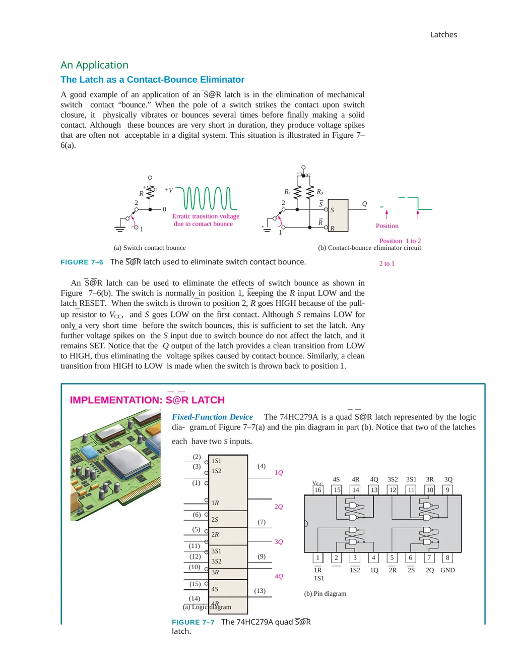
A good example of an application of an S@R latch is in the elimination of mechanical switch contact “bounce.” When the pole of a switch strikes the contact upon switch closure, it physically vibrates or bounces several times before finally making a solid contact. Although these bounces are very short in duration, they produce voltage spikes that are often not acceptable in a digital system. This situation is illustrated in Figure 7–6(a).
+VCC
+VCC R 2 Position Position 1 to 2 2 to 1 Erratic transition voltage due to contact bounce (a) Switch contact bounce (b) Contact-bounce eliminator circuit
FIGURE 7–6 The S@R latch used to eliminate switch contact bounce.
An S@R latch can be used to eliminate the effects of switch bounce as shown in Figure 7–6(b). The switch is normally in position 1, keeping the R input LOW and the latch RESET. When the switch is thrown to position 2, R goes HIGH because of the pull-up resistor to VCC, and S goes LOW on the first contact. Although S remains LOW for only a very short time before the switch bounces, this is sufficient to set the latch. Any further voltage spikes on the S input due to switch bounce do not affect the latch, and it remains SET. Notice that the Q output of the latch provides a clean transition from LOW to HIGH, thus eliminating the voltage spikes caused by contact bounce. Similarly, a clean transition from HIGH to LOW is made when the switch is thrown back to position 1.
IMPLEMENTATION: S@R LATCH
Fixed-Function Device The 74HC279A is a quad S@R latch represented by the logic dia- gram of Figure 7–7(a) and the pin diagram in part (b). Notice that two of the latches each have two S inputs. 1Q 3Q 4Q 2Q 16 15 14 13 12 11 10 9 1 2 3 4 5 6 7 8 VCC 4S 4R 4Q 3S2 3S1 3R 3Q 1S2 1Q 2R 2S 2Q GND 1R 1S1
(b) Pin diagram (a) Logic diagram
FIGURE 7–7 The 74HC279A quad S@R latch.<br>
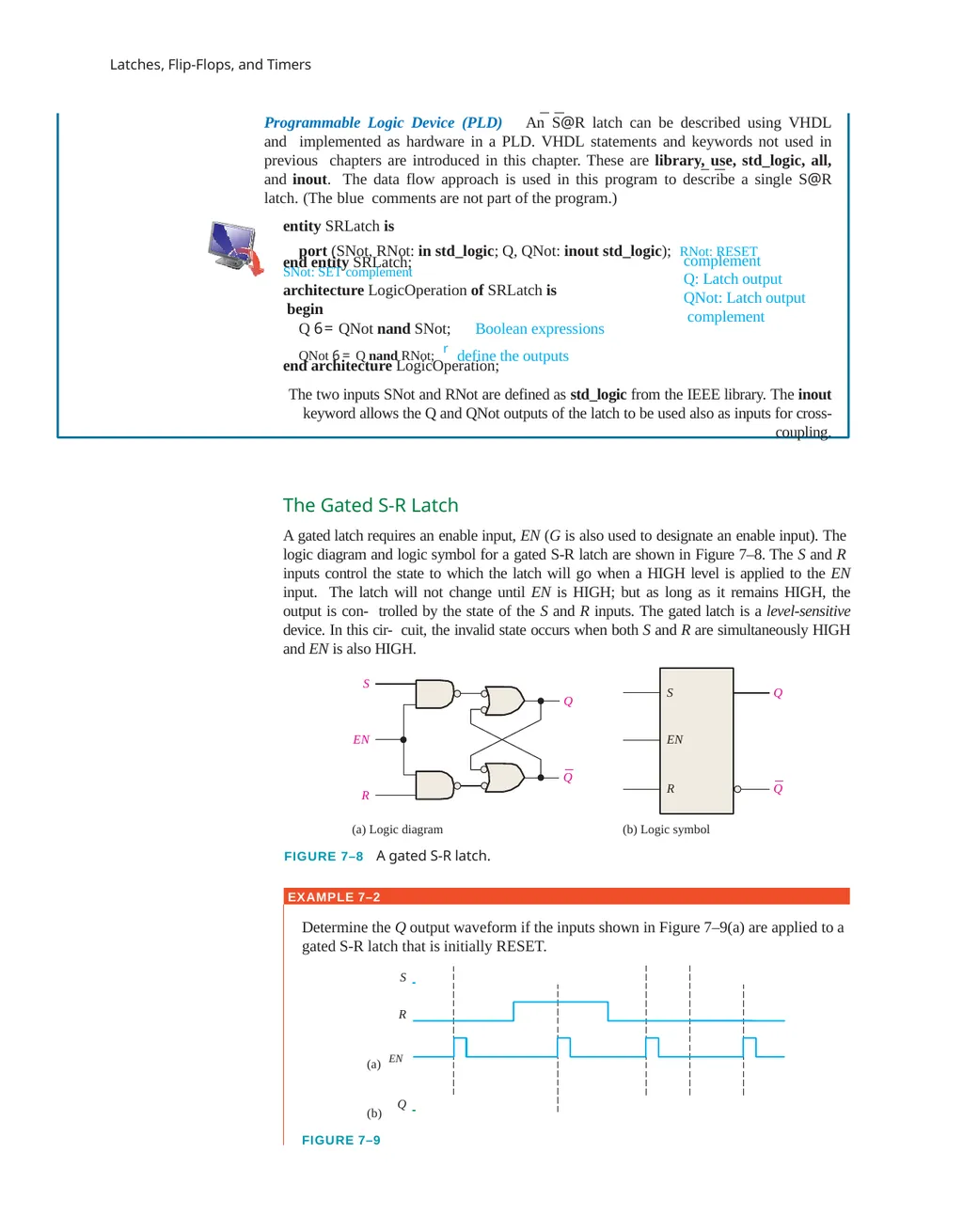
slide7. EXAMPLE 7–2 Q (b) Determine the Q output waveform if the inputs shown in Figure 7–9(a) are applied to a gated S-R latch that is initially RESET.
S
R
(a) EN FIGURE 7–9 S Q R Q (b) Logic symbol EN S R EN Q Q (a) Logic diagram FIGURE 7–8 A gated S-R latch. The Gated S-R Latch
A gated latch requires an enable input, EN (G is also used to designate an enable input). The logic diagram and logic symbol for a gated S-R latch are shown in Figure 7–8. The S and R inputs control the state to which the latch will go when a HIGH level is applied to the EN input. The latch will not change until EN is HIGH; but as long as it remains HIGH, the output is con- trolled by the state of the S and R inputs. The gated latch is a level-sensitive device. In this cir- cuit, the invalid state occurs when both S and R are simultaneously HIGH and EN is also HIGH. end entity SRLatch;
architecture LogicOperation of SRLatch is begin
Q 6= QNot nand SNot; end architecture LogicOperation;
The two inputs SNot and RNot are defined as std_logic from the IEEE library. The inout
keyword allows the Q and QNot outputs of the latch to be used also as inputs for cross-coupling. Latches, Flip-Flops, and Timers
Programmable Logic Device (PLD) An S@R latch can be described using VHDL and implemented as hardware in a PLD. VHDL statements and keywords not used in previous chapters are introduced in this chapter. These are library, use, std_logic, all, and inout. The data flow approach is used in this program to describe a single S@R latch. (The blue comments are not part of the program.)
entity SRLatch is SNot: SET complement port (SNot, RNot: in std_logic; Q, QNot: inout std_logic); RNot: RESET complement
Q: Latch output
QNot: Latch output complement Boolean expressions QNot 6= Q nand RNot; r define the outputs<br>
slide8. Latches Solution
The Q waveform is shown in Figure 7–9(b). When S is HIGH and R is LOW, a HIGH on the EN input sets the latch. When S is LOW and R is HIGH, a HIGH on the EN input resets the latch. When both S and R are LOW, the Q output does not change from its present state.
Related Problem
Determine the Q output of a gated S-R latch if the S and R inputs in Figure 7–9(a) are inverted.
The Gated D Latch
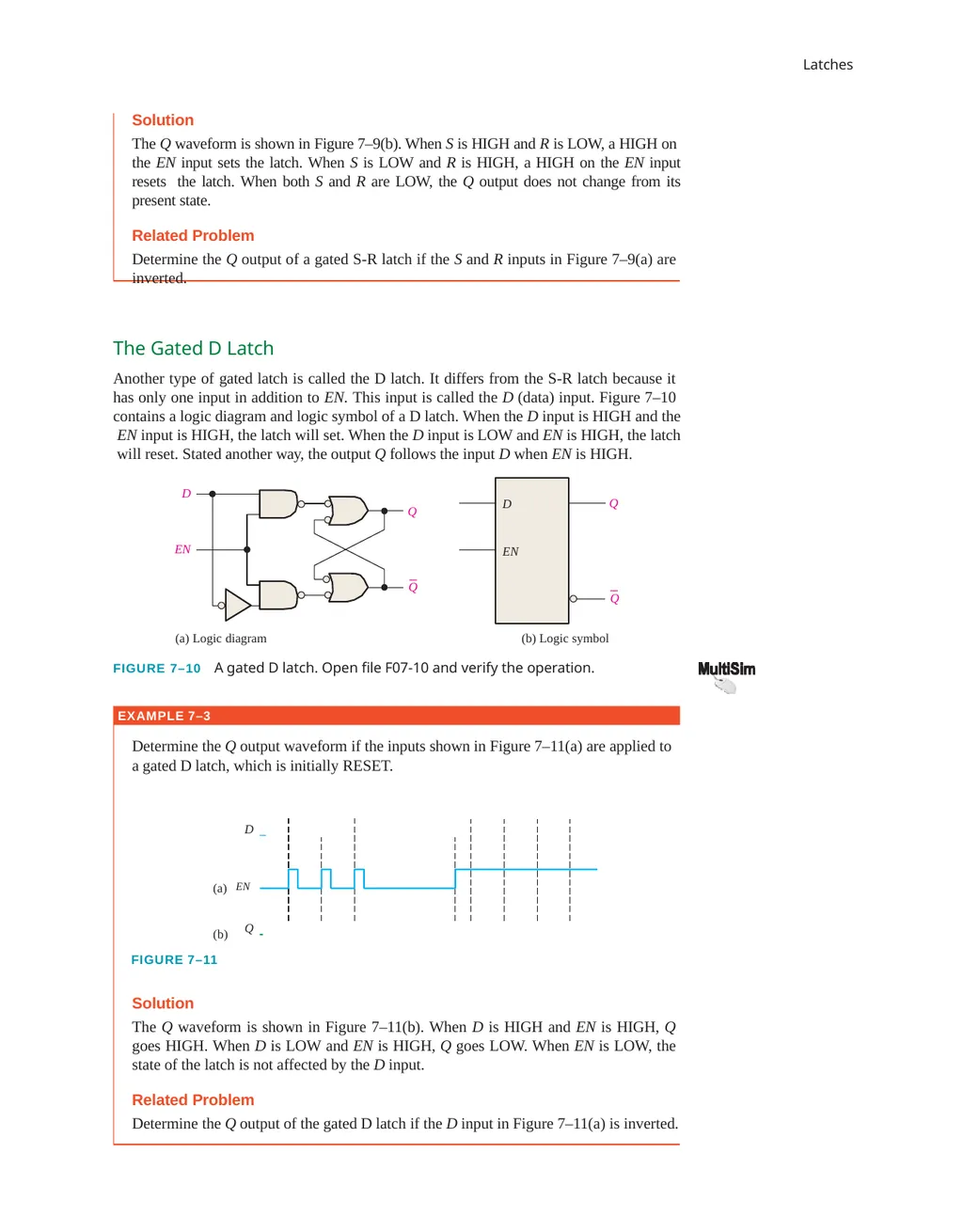
Another type of gated latch is called the D latch. It differs from the S-R latch because it has only one input in addition to EN. This input is called the D (data) input. Figure 7–10 contains a logic diagram and logic symbol of a D latch. When the D input is HIGH and the EN input is HIGH, the latch will set. When the D input is LOW and EN is HIGH, the latch will reset. Stated another way, the output Q follows the input D when EN is HIGH. EXAMPLE 7–3
Determine the Q output waveform if the inputs shown in Figure 7–11(a) are applied to a gated D latch, which is initially RESET. D Q (b) (a) EN FIGURE 7–11
Solution
The Q waveform is shown in Figure 7–11(b). When D is HIGH and EN is HIGH, Q goes HIGH. When D is LOW and EN is HIGH, Q goes LOW. When EN is LOW, the state of the latch is not affected by the D input.
Related Problem
Determine the Q output of the gated D latch if the D input in Figure 7–11(a) is inverted. D Q EN D EN Q Q Q
(a) Logic diagram (b) Logic symbol
FIGURE 7–10 A gated D latch. Open file F07-10 and verify the operation.<br>
slide9. Latches, Flip-Flops, and Timers SECTION 7–1 CHECKUP Answers are at the end of the chapter.
List three types of latches.
Develop the truth table for the active-HIGH input S-R latch in Figure 7–1(a).
What is the Q output of a D latch when EN = 1 and D = 1? IMPLEMENTATION: GATED D LATCH
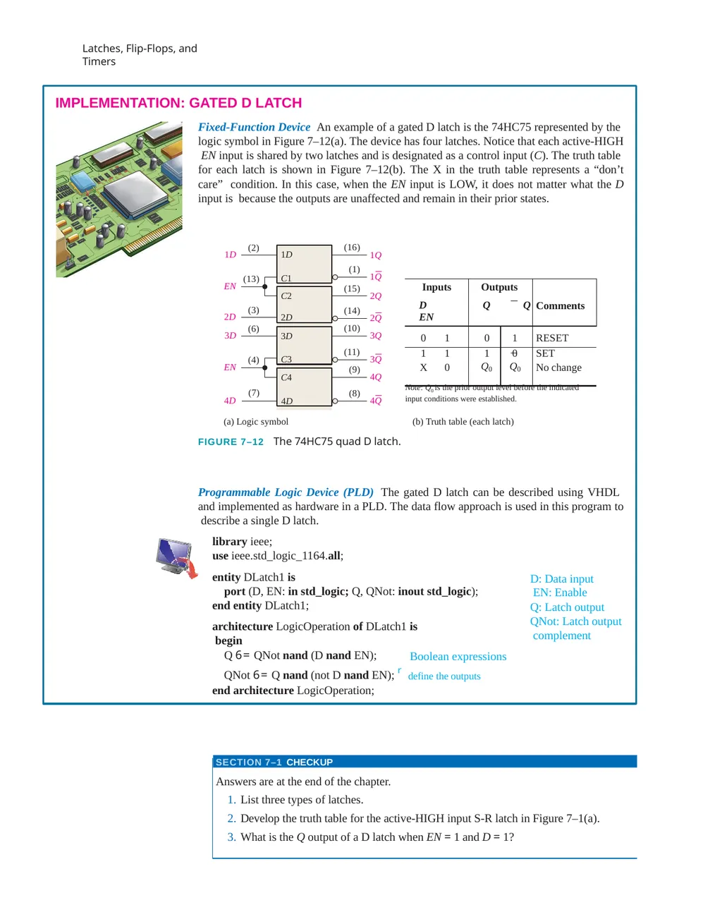
Fixed-Function Device An example of a gated D latch is the 74HC75 represented by the logic symbol in Figure 7–12(a). The device has four latches. Notice that each active-HIGH EN input is shared by two latches and is designated as a control input (C). The truth table for each latch is shown in Figure 7–12(b). The X in the truth table represents a “don’t care” condition. In this case, when the EN input is LOW, it does not matter what the D input is because the outputs are unaffected and remain in their prior states. Programmable Logic Device (PLD) The gated D latch can be described using VHDL and implemented as hardware in a PLD. The data flow approach is used in this program to describe a single D latch.
library ieee;
use ieee.std_logic_1164.all; entity DLatch1 is
port (D, EN: in std_logic; Q, QNot: inout std_logic); end entity DLatch1;
architecture LogicOperation of DLatch1 is begin
Q 6= QNot nand (D nand EN); (13) (14) (a) Logic symbol (b) Truth table (each latch) 2Q
3Q (10) 1D 1Q (16) (1) 1Q 2Q (15) (11) 3Q
4Q (9) (8) 4Q (2) EN 1D
C1 (4) 3D (6) EN 3D
C3 C4
4D 4D (7) C2
2D 2D (3) Note: Q0 is the prior output level before the indicated input conditions were established. FIGURE 7–12 The 74HC75 quad D latch. Boolean expressions QNot 6= Q nand (not D nand EN); r define the outputs
end architecture LogicOperation; D: Data input EN: Enable
Q: Latch output QNot: Latch output complement<br>
slide10. Flip-Flops 7–2 Flip-Flops Flip-flops are synchronous bistable devices, also known as bistable multivibrators. In this case, the term synchronous means that the output changes state only at a specified point (leading or trailing edge) on the triggering input called the clock (CLK), which is designated as a control input, C; that is, changes in the output occur in synchronization with the clock. Flip-flops are edge-triggered or edge-sensitive whereas gated latches are level-sensitive.
After completing this section, you should be able to ◆ Define clock
Define edge-triggered flip-flop
Explain the difference between a flip-flop and a latch Identify an edge-triggered flip-flop by its logic symbol
Discuss the difference between a positive and a negative edge-triggered flip-flop
Discuss and compare the operation of D and J-K edge-triggered flip-flops and ex- plain the differences in their truth tables
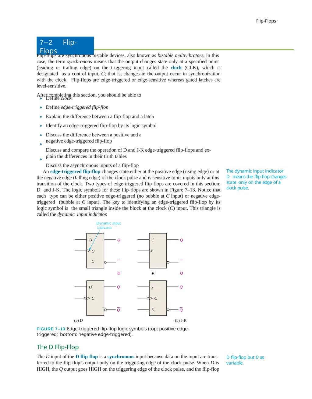
Discuss the asynchronous inputs of a flip-flop ◆ ◆ ◆ ◆ ◆ ◆ The dynamic input indicator D means the flip-flop changes state only on the edge of a clock pulse. An edge-triggered flip-flop changes state either at the positive edge (rising edge) or at the negative edge (falling edge) of the clock pulse and is sensitive to its inputs only at this transition of the clock. Two types of edge-triggered flip-flops are covered in this section: D and J-K. The logic symbols for these flip-flops are shown in Figure 7–13. Notice that each type can be either positive edge-triggered (no bubble at C input) or negative edge-triggered (bubble at C input). The key to identifying an edge-triggered flip-flop by its logic symbol is the small triangle inside the block at the clock (C) input. This triangle is called the dynamic input indicator.
Dynamic input indicator
D Q J Q
C C
Q K Q D Q Q C J Q K Q C (a) D (b) J-K
FIGURE 7–13 Edge-triggered flip-flop logic symbols (top: positive edge-triggered; bottom: negative edge-triggered). The D Flip-Flop
The D input of the D flip-flop is a synchronous input because data on the input are trans- ferred to the flip-flop’s output only on the triggering edge of the clock pulse. When D is HIGH, the Q output goes HIGH on the triggering edge of the clock pulse, and the flip-flop D flip-flop but D as variable.<br>
slide11. Latches, Flip-Flops, and Timers is SET. When D is LOW, the Q output goes LOW on the triggering edge of the clock pulse, and the flip-flop is RESET.
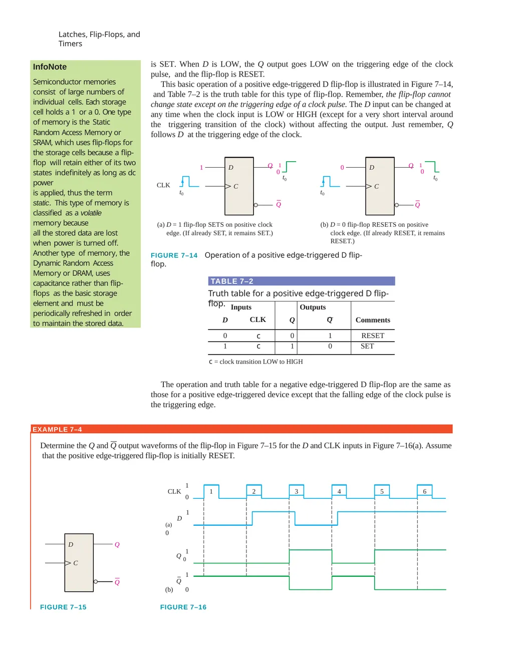
This basic operation of a positive edge-triggered D flip-flop is illustrated in Figure 7–14, and Table 7–2 is the truth table for this type of flip-flop. Remember, the flip-flop cannot change state except on the triggering edge of a clock pulse. The D input can be changed at any time when the clock input is LOW or HIGH (except for a very short interval around the triggering transition of the clock) without affecting the output. Just remember, Q follows D at the triggering edge of the clock. InfoNote
Semiconductor memories consist of large numbers of individual cells. Each storage cell holds a 1 or a 0. One type of memory is the Static Random Access Memory or SRAM, which uses flip-flops for
the storage cells because a flip-flop will retain either of its two states indefinitely as long as dc power
is applied, thus the term static. This type of memory is classified as a volatile memory because
all the stored data are lost when power is turned off. Another type of memory, the Dynamic Random Access Memory or DRAM, uses capacitance rather than flip-flops as the basic storage element and must be periodically refreshed in order to maintain the stored data. D (a) D = 1 flip-flop SETS on positive clock edge. (If already SET, it remains SET.) C t0 1 CLK t0 Q 1 0 D (b) D = 0 flip-flop RESETS on positive
clock edge. (If already RESET, it remains RESET.) C t0 0 t0 Q 1 0 Q Q FIGURE 7–14 Operation of a positive edge-triggered D flip-flop. TABLE 7–2 Truth table for a positive edge-triggered D flip-flop. c = clock transition LOW to HIGH
The operation and truth table for a negative edge-triggered D flip-flop are the same as those for a positive edge-triggered device except that the falling edge of the clock pulse is the triggering edge. D Q Q C FIGURE 7–15 1
D
(a) 0 (b) 1
Q 0
1
Q
0 CLK 1
0 1 2 3 4 5 6 FIGURE 7–16 EXAMPLE 7–4 Determine the Q and Q output waveforms of the flip-flop in Figure 7–15 for the D and CLK inputs in Figure 7–16(a). Assume that the positive edge-triggered flip-flop is initially RESET.<br>
slide12. The J-K Flip-Flop
The J and K inputs of the J-K flip-flop are synchronous inputs because data on these inputs are transferred to the flip-flop’s output only on the triggering edge of the clock pulse. When J is HIGH and K is LOW, the Q output goes HIGH on the triggering edge of the clock pulse, and the flip-flop is SET. When J is LOW and K is HIGH, the Q output goes LOW on the triggering edge of the clock pulse, and the flip-flop is RESET. When both J and K are LOW, the output does not change from its prior state. When J and K are both HIGH, the flip-flop changes state. This called the toggle mode.
This basic operation of a positive edge-triggered flip-flop is illustrated in Figure 7–17, and Table 7–3 is the truth table for this type of flip-flop. Remember, the flip-flop cannot change state except on the triggering edge of a clock pulse. The J and K inputs can be changed at any time when the clock input is LOW or HIGH (except for a very short interval around the triggering transition of the clock) without affecting the output. Flip-Flops
Solution
At clock pulse 1, D is LOW, so Q remains LOW (RESET).
At clock pulse 2, D is LOW, so Q remains LOW (RESET).
At clock pulse 3, D is HIGH, so Q goes HIGH (SET).
At clock pulse 4, D is LOW, so Q goes LOW (RESET).
At clock pulse 5, D is HIGH, so Q goes HIGH (SET).
At clock pulse 6, D is HIGH, so Q remains HIGH (SET).
Once Q is determined, Q is easily found since it is simply the complement of Q. The resulting waveforms for Q and Q are shown in Figure 7–16(b) for the input waveforms in part (a).
Related Problem
Determine Q and Q for the D input in Figure 7–16(a) if the flip-flop is a negative edge-triggered device. J C t0 1 CLK t0 Q 1 0 0 K Q
(a) J = 1, K = 0 flip-flop SETS on positive clock edge. (If already SET, it remains SET.) J C t0 0 t0 Q 1
0 1 K Q
(b) J = 0, K = 1 flip-flop RESETS on positive clock edge. (If already RESET, it remains RESET.) J Q = Q0 (no change) C 0 K Q
(d) J = 0, K = 0 flip-flop does not change. (If SET, it remains SET; if RESET, it remains RESET.) t0 0 J Q C 1 K
(c) J = 1, K = 1 flip-flop changes state (toggle). t0 1 Q Q Q FIGURE 7–17 Operation of a positive edge-triggered J-K flip-flop.<br>
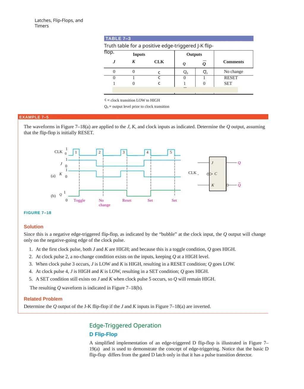
slide13. Latches, Flip-Flops, and Timers TABLE 7–3 Truth table for a positive edge-triggered J-K flip-flop. c = clock transition LOW to HIGH
Q0 = output level prior to clock transition EXAMPLE 7–5 The waveforms in Figure 7–18(a) are applied to the J, K, and clock inputs as indicated. Determine the Q output, assuming that the flip-flop is initially RESET. (a) (b) 1 2 3 4 5 1
CLK 0 1
J 0 1
K 0 Q 1
0 Toggle No change Reset Set Set J Q Q C K CLK FIGURE 7–18
Solution
Since this is a negative edge-triggered flip-flop, as indicated by the “bubble” at the clock input, the Q output will change only on the negative-going edge of the clock pulse.
At the first clock pulse, both J and K are HIGH; and because this is a toggle condition, Q goes HIGH.
At clock pulse 2, a no-change condition exists on the inputs, keeping Q at a HIGH level.
When clock pulse 3 occurs, J is LOW and K is HIGH, resulting in a RESET condition; Q goes LOW.
At clock pulse 4, J is HIGH and K is LOW, resulting in a SET condition; Q goes HIGH.
A SET condition still exists on J and K when clock pulse 5 occurs, so Q will remain HIGH.
The resulting Q waveform is indicated in Figure 7–18(b).
Related Problem
Determine the Q output of the J-K flip-flop if the J and K inputs in Figure 7–18(a) are inverted.
Edge-Triggered Operation
D Flip-Flop
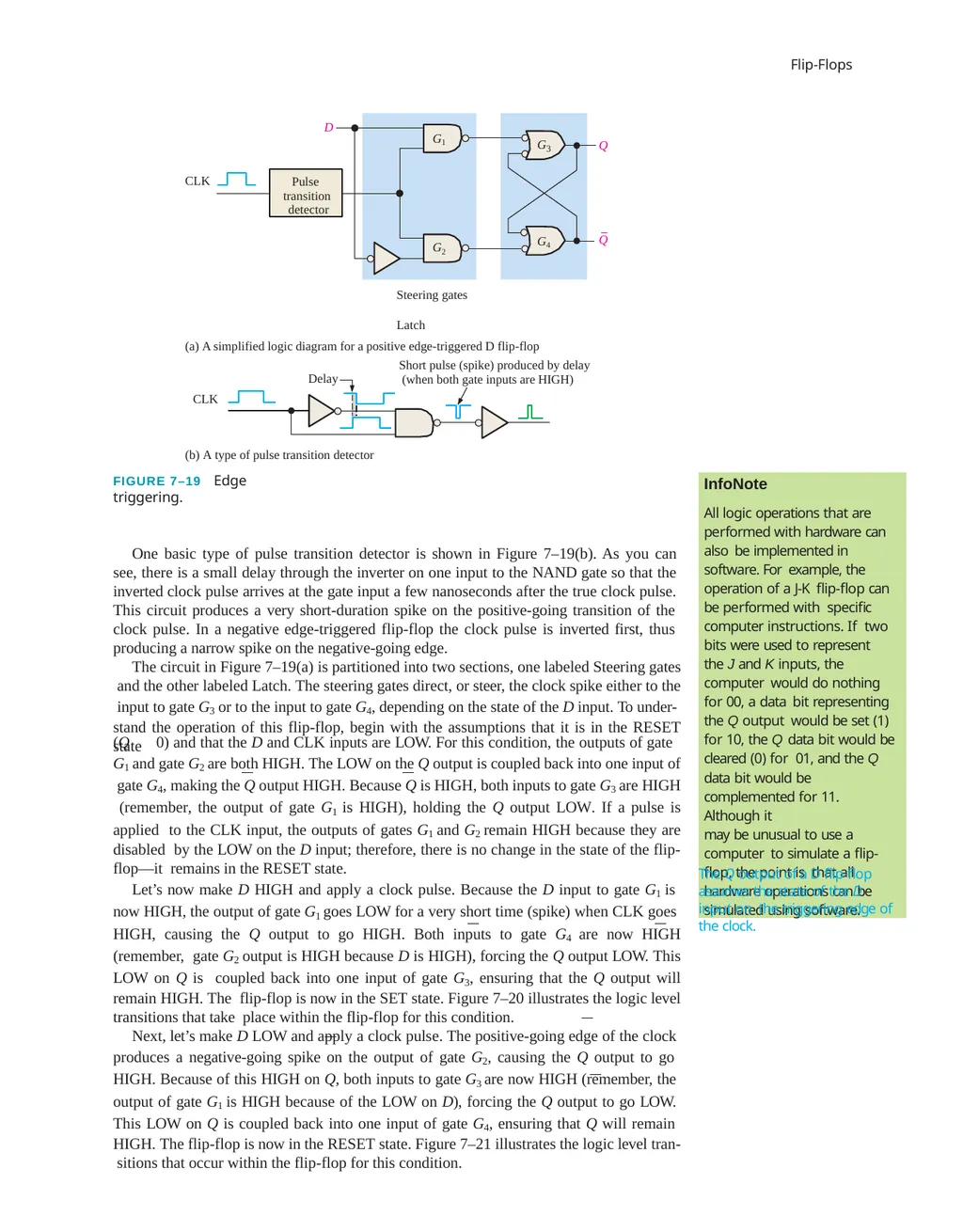
A simplified implementation of an edge-triggered D flip-flop is illustrated in Figure 7–19(a) and is used to demonstrate the concept of edge-triggering. Notice that the basic D flip-flop differs from the gated D latch only in that it has a pulse transition detector.<br>
slide14. Flip-Flops One basic type of pulse transition detector is shown in Figure 7–19(b). As you can see, there is a small delay through the inverter on one input to the NAND gate so that the inverted clock pulse arrives at the gate input a few nanoseconds after the true clock pulse. This circuit produces a very short-duration spike on the positive-going transition of the clock pulse. In a negative edge-triggered flip-flop the clock pulse is inverted first, thus producing a narrow spike on the negative-going edge.
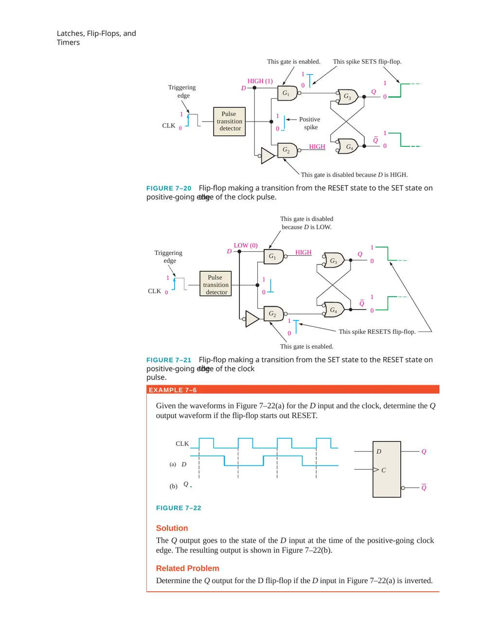
The circuit in Figure 7–19(a) is partitioned into two sections, one labeled Steering gates and the other labeled Latch. The steering gates direct, or steer, the clock spike either to the input to gate G3 or to the input to gate G4, depending on the state of the D input. To under- stand the operation of this flip-flop, begin with the assumptions that it is in the RESET state (Q 0) and that the D and CLK inputs are LOW. For this condition, the outputs of gate G1 and gate G2 are both HIGH. The LOW on the Q output is coupled back into one input of gate G4, making the Q output HIGH. Because Q is HIGH, both inputs to gate G3 are HIGH (remember, the output of gate G1 is HIGH), holding the Q output LOW. If a pulse is applied to the CLK input, the outputs of gates G1 and G2 remain HIGH because they are disabled by the LOW on the D input; therefore, there is no change in the state of the flip-flop—it remains in the RESET state.
Let’s now make D HIGH and apply a clock pulse. Because the D input to gate G1 is now HIGH, the output of gate G1 goes LOW for a very short time (spike) when CLK goes HIGH, causing the Q output to go HIGH. Both inputs to gate G4 are now HIGH (remember, gate G2 output is HIGH because D is HIGH), forcing the Q output LOW. This LOW on Q is coupled back into one input of gate G3, ensuring that the Q output will remain HIGH. The flip-flop is now in the SET state. Figure 7–20 illustrates the logic level transitions that take place within the flip-flop for this condition.
Next, let’s make D LOW and apply a clock pulse. The positive-going edge of the clock produces a negative-going spike on the output of gate G2, causing the Q output to go HIGH. Because of this HIGH on Q, both inputs to gate G3 are now HIGH (remember, the output of gate G1 is HIGH because of the LOW on D), forcing the Q output to go LOW. This LOW on Q is coupled back into one input of gate G4, ensuring that Q will remain HIGH. The flip-flop is now in the RESET state. Figure 7–21 illustrates the logic level tran- sitions that occur within the flip-flop for this condition. G1 G2 G 3 G4 CLK (b) A type of pulse transition detector Steering gates Latch
(a) A simplified logic diagram for a positive edge-triggered D flip-flop Delay Q D Q CLK Pulse transition detector Short pulse (spike) produced by delay (when both gate inputs are HIGH) FIGURE 7–19 Edge triggering. InfoNote
All logic operations that are performed with hardware can also be implemented in software. For example, the operation of a J-K flip-flop can be performed with specific computer instructions. If two bits were used to represent the J and K inputs, the computer would do nothing for 00, a data bit representing the Q output would be set (1) for 10, the Q data bit would be cleared (0) for 01, and the Q data bit would be complemented for 11. Although it
may be unusual to use a computer to simulate a flip-flop, the point is that all hardware operations can be simulated using software. The Q output of a D flip-flop assumes the state of the D input on the triggering edge of the clock.<br>
slide15. Latches, Flip-Flops, and Timers Q Q This gate is enabled. HIGH (1)
D Triggering edge This spike SETS flip-flop. This gate is disabled because D is HIGH. 0 1 Positive spike G1 G 2 G 3 HIGH G4 0 1 0 1 1
0 1
CLK 0 Pulse transition detector FIGURE 7–20 Flip-flop making a transition from the RESET state to the SET state on the Triggering edge This gate is enabled. D Q Q LOW (0) This spike RESETS flip-flop. 0 1 HIGH G 1 G 2 G3 G4 Pulse transition detector 1
CLK 0 0 1 0 1 1
0 positive-going edge of the clock pulse.
This gate is disabled because D is LOW. FIGURE 7–21 Flip-flop making a transition from the SET state to the RESET state on the positive-going edge of the clock pulse. EXAMPLE 7–6 Given the waveforms in Figure 7–22(a) for the D input and the clock, determine the Q
output waveform if the flip-flop starts out RESET. CLK (a) D Q (b) D Q Q C FIGURE 7–22
Solution
The Q output goes to the state of the D input at the time of the positive-going clock edge. The resulting output is shown in Figure 7–22(b).
Related Problem
Determine the Q output for the D flip-flop if the D input in Figure 7–22(a) is inverted.<br>
slide16. Flip-Flops J-K Flip-Flop
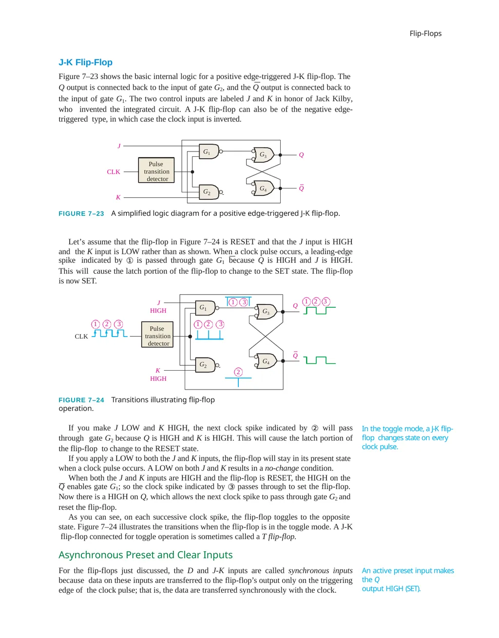
Figure 7–23 shows the basic internal logic for a positive edge-triggered J-K flip-flop. The Q output is connected back to the input of gate G2, and the Q output is connected back to the input of gate G1. The two control inputs are labeled J and K in honor of Jack Kilby, who invented the integrated circuit. A J-K flip-flop can also be of the negative edge-triggered type, in which case the clock input is inverted. K J Q Q Pulse transition detector CLK G1 G 2 G3 G4 FIGURE 7–23 A simplified logic diagram for a positive edge-triggered J-K flip-flop.
Let’s assume that the flip-flop in Figure 7–24 is RESET and that the J input is HIGH and the K input is LOW rather than as shown. When a clock pulse occurs, a leading-edge spike indicated by ① is passed through gate G1 because Q is HIGH and J is HIGH. This will cause the latch portion of the flip-flop to change to the SET state. The flip-flop is now SET. If you make J LOW and K HIGH, the next clock spike indicated by ② will pass through gate G2 because Q is HIGH and K is HIGH. This will cause the latch portion of the flip-flop to change to the RESET state.
If you apply a LOW to both the J and K inputs, the flip-flop will stay in its present state when a clock pulse occurs. A LOW on both J and K results in a no-change condition.
When both the J and K inputs are HIGH and the flip-flop is RESET, the HIGH on the Q enables gate G1; so the clock spike indicated by ③ passes through to set the flip-flop. Now there is a HIGH on Q, which allows the next clock spike to pass through gate G2 and reset the flip-flop.
As you can see, on each successive clock spike, the flip-flop toggles to the opposite state. Figure 7–24 illustrates the transitions when the flip-flop is in the toggle mode. A J-K flip-flop connected for toggle operation is sometimes called a T flip-flop. Asynchronous Preset and Clear Inputs
For the flip-flops just discussed, the D and J-K inputs are called synchronous inputs because data on these inputs are transferred to the flip-flop’s output only on the triggering edge of the clock pulse; that is, the data are transferred synchronously with the clock. K J Q Q G 1 G 2 G3 G4 Pulse transition detector 1 3 CLK 1 2 3 1 2 3 2 HIGH 1 2 3 HIGH
FIGURE 7–24 Transitions illustrating flip-flop operation. In the toggle mode, a J-K flip-flop changes state on every clock pulse. An active preset input makes the Q
output HIGH (SET).<br>
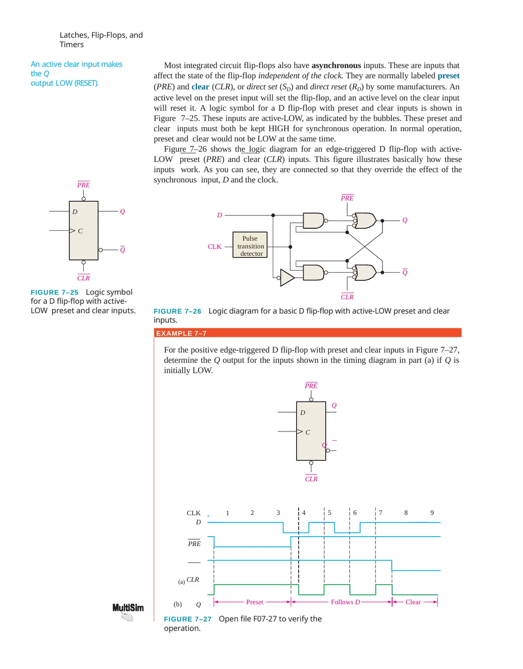
slide17. Latches, Flip-Flops, and Timers Most integrated circuit flip-flops also have asynchronous inputs. These are inputs that affect the state of the flip-flop independent of the clock. They are normally labeled preset (PRE) and clear (CLR), or direct set (SD) and direct reset (RD) by some manufacturers. An active level on the preset input will set the flip-flop, and an active level on the clear input will reset it. A logic symbol for a D flip-flop with preset and clear inputs is shown in Figure 7–25. These inputs are active-LOW, as indicated by the bubbles. These preset and clear inputs must both be kept HIGH for synchronous operation. In normal operation, preset and clear would not be LOW at the same time.
Figure 7–26 shows the logic diagram for an edge-triggered D flip-flop with active-LOW preset (PRE) and clear (CLR) inputs. This figure illustrates basically how these inputs work. As you can see, they are connected so that they override the effect of the synchronous input, D and the clock. D Q Q C PRE CLR FIGURE 7–25 Logic symbol for a D flip-flop with active-LOW preset and clear inputs. D Q Q Pulse transition detector CLK PRE CLR FIGURE 7–26 Logic diagram for a basic D flip-flop with active-LOW preset and clear inputs. An active clear input makes the Q
output LOW (RESET). EXAMPLE 7–7 For the positive edge-triggered D flip-flop with preset and clear inputs in Figure 7–27, determine the Q output for the inputs shown in the timing diagram in part (a) if Q is initially LOW.
PRE
Q
D
C
Q CLR (b) 2 3 4 5 CLK 1 6 7 8 9 Clear D
PRE
(a) CLR Q Preset Follows D FIGURE 7–27 Open file F07-27 to verify the operation.<br>
slide18. Flip-Flops Solution
During clock pulses 1, 2, and 3, the preset (PRE) is LOW, keeping the flip-flop SET regardless of the synchronous D input.
For clock pulses 4, 5, 6, and 7, the output follows the input on the clock pulse because both PRE and CLR are HIGH.
For clock pulses 8 and 9, the clear (CLR) input is LOW, keeping the flip-flop RESET regardless of the synchronous inputs.
The resulting Q output is shown in Figure 7–27(b).
Related Problem
If you interchange the PRE and CLR waveforms in Figure 7–27(a), what will the Q
output look like? Let’s look at two specific edge-triggered flip-flops. They are representative of the vari- ous types of flip-flops available in fixed-function IC form and, like most other devices, are available in CMOS and in bipolar (TTL) logic families.
Also, you will learn how VHDL is used to describe the types of flip-flops. IMPLEMENTATION: D FLIP-FLOP
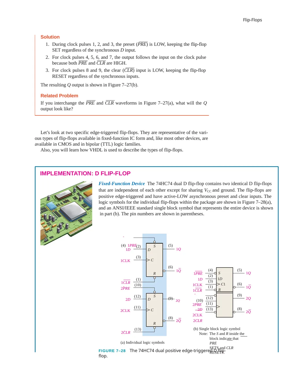
Fixed-Function Device The 74HC74 dual D flip-flop contains two identical D flip-flops that are independent of each other except for sharing VCC and ground. The flip-flops are positive edge-triggered and have active-LOW asynchronous preset and clear inputs. The logic symbols for the individual flip-flops within the package are shown in Figure 7–28(a), and an ANSI/IEEE standard single block symbol that represents the entire device is shown in part (b). The pin numbers are shown in parentheses. (11) D C 1CLR (6)
1Q 1D 1CLK (5)
1Q (3) (2) (4) 1PRE (1) D 2Q C 2PRE 2CLR (8) 2D 2CLK (9) 2Q (11) (12) (10) (13) (8) (3) (2) (4) (1) (12) (13) (5) (6) (9) 1PRE
1D
1CLK 1Q 1CLR (10) 2PRE
2D
2CLK
2CLR 1Q 2Q 2Q S
1D
C1
R (b) Single block logic symbol Note: The S and R inside the
block indicate that PRE
SETS and CLR RESETS. (a) Individual logic symbols S R S R FIGURE 7–28 The 74HC74 dual positive edge-triggered D flip-flop.<br>
slide19. Latches, Flip-Flops, and Timers
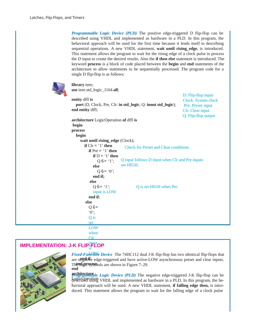
Programmable Logic Device (PLD) The positive edge-triggered D flip-flop can be described using VHDL and implemented as hardware in a PLD. In this program, the behavioral approach will be used for the first time because it lends itself to describing sequential operations. A new VHDL statement, wait until rising_edge, is introduced. This statement allows the program to wait for the rising edge of a clock pulse to process the D input to create the desired results. Also the if then else statement is introduced. The keyword process is a block of code placed between the begin and end statements of the architecture to allow statements to be sequentially processed. The program code for a single D flip-flop is as follows:
library ieee;
use ieee.std_logic_1164.all; entity dffl is
port (D, Clock, Pre, Clr: in std_logic; Q: inout std_logic); end entity dffl; architecture LogicOperation of dffl is begin
process
begin
wait until rising_edge (Clock); if Clr = ‘1’ then
if Pre = ‘1’ then if D = ‘1’ then
Q 6= ‘1’;
else
Q 6= ‘0’;
end if; else D: Flip-flop input Clock: System clock Pre: Preset input Clr: Clear input
Q: Flip-flop output Q 6= ‘1’; Q is set HIGH when Pre input is LOW.
end if; else
Q 6= ‘0’; Q is set LOW when Clr input is LOW.
end if; end process;
end architecture LogicOperation; Check for Preset and Clear conditions Q input follows D input when Clr and Pre inputs are HIGH. IMPLEMENTATION: J-K FLIP-FLOP
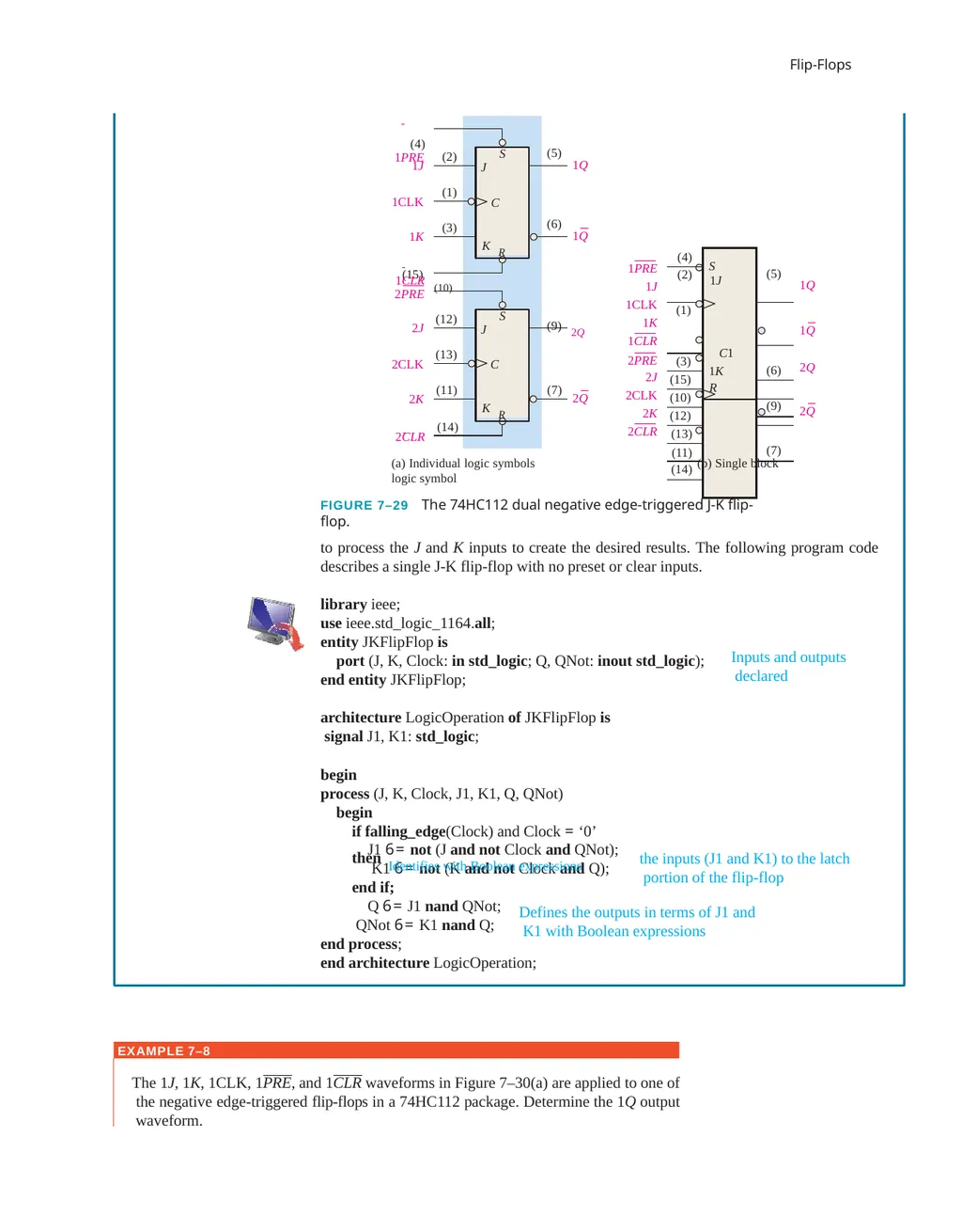
Fixed-Function Device The 74HC112 dual J-K flip-flop has two identical flip-flops that are negative edge-triggered and have active-LOW asynchronous preset and clear inputs. The logic symbols are shown in Figure 7–29.
Programmable Logic Device (PLD) The negative edge-triggered J-K flip-flop can be described using VHDL and implemented as hardware in a PLD. In this program, the be- havioral approach will be used. A new VHDL statement, if falling edge then, is intro- duced. This statement allows the program to wait for the falling edge of a clock pulse<br>
slide20. Flip-Flops to process the J and K inputs to create the desired results. The following program code describes a single J-K flip-flop with no preset or clear inputs. library ieee;
use ieee.std_logic_1164.all;
entity JKFlipFlop is
port (J, K, Clock: in std_logic; Q, QNot: inout std_logic); end entity JKFlipFlop; J1 6= not (J and not Clock and QNot); K1 6= not (K and not Clock and Q);
end if; Q 6= J1 nand QNot; QNot 6= K1 nand Q;
end process; end architecture LogicOperation; Inputs and outputs declared Defines the outputs in terms of J1 and K1 with Boolean expressions architecture LogicOperation of JKFlipFlop is signal J1, K1: std_logic;
begin
process (J, K, Clock, J1, K1, Q, QNot)
begin
if falling_edge(Clock) and Clock = ‘0’ then Identifies with Boolean expressions the inputs (J1 and K1) to the latch portion of the flip-flop (6)
1Q 1J 1CLK (5)
1Q (1) (2) (4) 1PRE 2Q 2PRE 2CLR (7) 2CLK (9) 2Q (13) 2J (12) (15)
1CLR (10) (14) 1Q 1Q 2Q 2Q 1K (3) 2K (11) 1PRE
1J
1CLK
1K
1CLR
2PRE
2J
2CLK
2K
2CLR S
J
C
K R S
J
C
K R (a) Individual logic symbols (b) Single block logic symbol
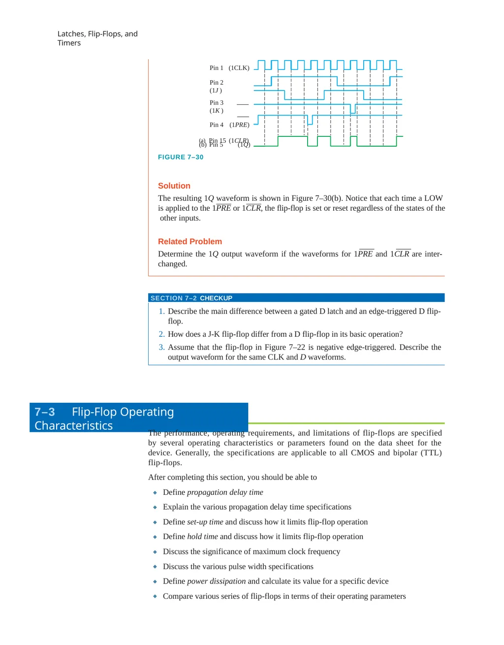
FIGURE 7–29 The 74HC112 dual negative edge-triggered J-K flip-flop. EXAMPLE 7–8 The 1J, 1K, 1CLK, 1PRE, and 1CLR waveforms in Figure 7–30(a) are applied to one of the negative edge-triggered flip-flops in a 74HC112 package. Determine the 1Q output waveform.<br>
slide21. Latches, Flip-Flops, and Timers Solution
The resulting 1Q waveform is shown in Figure 7–30(b). Notice that each time a LOW is applied to the 1PRE or 1CLR, the flip-flop is set or reset regardless of the states of the other inputs.
Related Problem
Determine the 1Q output waveform if the waveforms for 1PRE and 1CLR are inter- changed. (1Q) Pin 1 (1CLK)
Pin 2 (1J )
Pin 3 (1K )
Pin 4 (1PRE)
(a) Pin 15 (1CLR) (b) Pin 5
FIGURE 7–30 SECTION 7–2 CHECKUP Describe the main difference between a gated D latch and an edge-triggered D flip- flop.
How does a J-K flip-flop differ from a D flip-flop in its basic operation?
Assume that the flip-flop in Figure 7–22 is negative edge-triggered. Describe the output waveform for the same CLK and D waveforms. 7–3 Flip-Flop Operating Characteristics The performance, operating requirements, and limitations of flip-flops are specified by several operating characteristics or parameters found on the data sheet for the device. Generally, the specifications are applicable to all CMOS and bipolar (TTL) flip-flops.
After completing this section, you should be able to ◆ Define propagation delay time
Explain the various propagation delay time specifications Define set-up time and discuss how it limits flip-flop operation Define hold time and discuss how it limits flip-flop operation Discuss the significance of maximum clock frequency
Discuss the various pulse width specifications
Define power dissipation and calculate its value for a specific device Compare various series of flip-flops in terms of their operating parameters ◆ ◆ ◆ ◆ ◆ ◆ ◆<br>
slide22. Flip-Flop Operating Characteristics
Propagation Delay Times
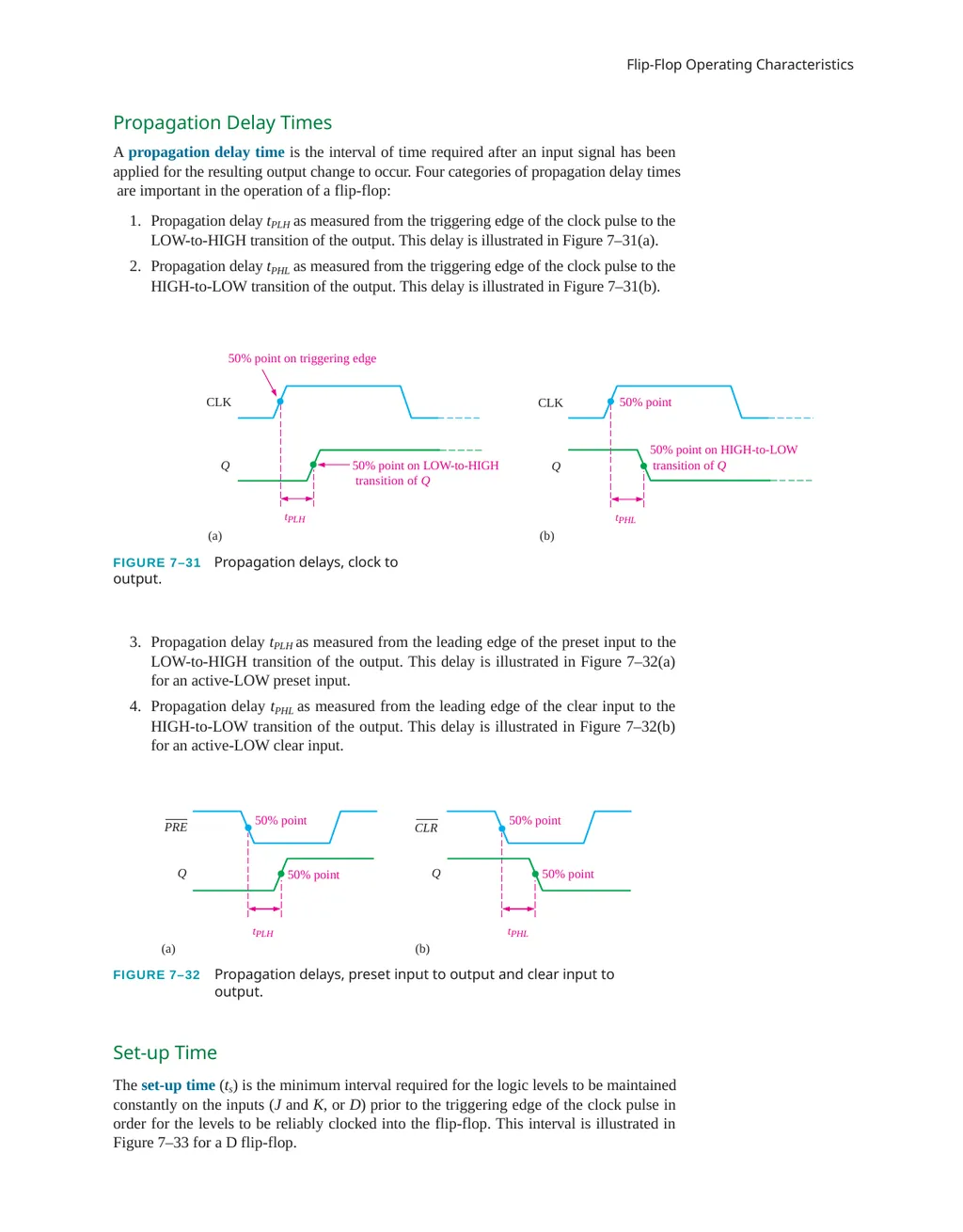
A propagation delay time is the interval of time required after an input signal has been applied for the resulting output change to occur. Four categories of propagation delay times are important in the operation of a flip-flop:
Propagation delay tPLH as measured from the triggering edge of the clock pulse to the LOW-to-HIGH transition of the output. This delay is illustrated in Figure 7–31(a).
Propagation delay tPHL as measured from the triggering edge of the clock pulse to the HIGH-to-LOW transition of the output. This delay is illustrated in Figure 7–31(b). 50% point on triggering edge 50% point on LOW-to-HIGH transition of Q tPLH CLK Q (a) tPHL Q CLK 50% point 50% point on HIGH-to-LOW transition of Q (b) FIGURE 7–31 Propagation delays, clock to output. Propagation delay tPLH as measured from the leading edge of the preset input to the LOW-to-HIGH transition of the output. This delay is illustrated in Figure 7–32(a) for an active-LOW preset input.
Propagation delay tPHL as measured from the leading edge of the clear input to the HIGH-to-LOW transition of the output. This delay is illustrated in Figure 7–32(b) for an active-LOW clear input. tPHL (a) (b) CLR Q 50% point tPLH Q PRE 50% point 50% point 50% point FIGURE 7–32 Propagation delays, preset input to output and clear input to output. Set-up Time
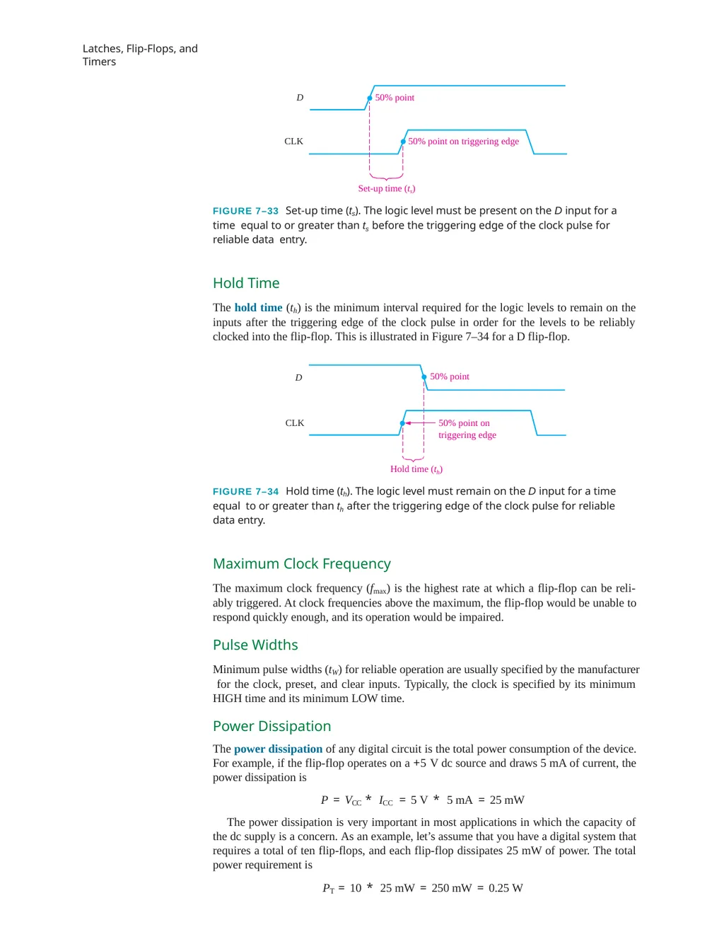
The set-up time (ts) is the minimum interval required for the logic levels to be maintained constantly on the inputs (J and K, or D) prior to the triggering edge of the clock pulse in order for the levels to be reliably clocked into the flip-flop. This interval is illustrated in Figure 7–33 for a D flip-flop.<br>
slide23. Latches, Flip-Flops, and Timers 50% point 50% point on triggering edge CLK D Set-up time (ts)
FIGURE 7–33 Set-up time (ts). The logic level must be present on the D input for a time equal to or greater than ts before the triggering edge of the clock pulse for reliable data entry.
Hold Time
The hold time (th) is the minimum interval required for the logic levels to remain on the inputs after the triggering edge of the clock pulse in order for the levels to be reliably clocked into the flip-flop. This is illustrated in Figure 7–34 for a D flip-flop. CLK D 50% point on triggering edge 50% point Hold time (th)
FIGURE 7–34 Hold time (th). The logic level must remain on the D input for a time equal to or greater than th after the triggering edge of the clock pulse for reliable data entry.
Maximum Clock Frequency
The maximum clock frequency (fmax) is the highest rate at which a flip-flop can be reli- ably triggered. At clock frequencies above the maximum, the flip-flop would be unable to respond quickly enough, and its operation would be impaired.
Pulse Widths
Minimum pulse widths (tW) for reliable operation are usually specified by the manufacturer for the clock, preset, and clear inputs. Typically, the clock is specified by its minimum HIGH time and its minimum LOW time.
Power Dissipation
The power dissipation of any digital circuit is the total power consumption of the device. For example, if the flip-flop operates on a +5 V dc source and draws 5 mA of current, the power dissipation is
P = VCC * ICC = 5 V * 5 mA = 25 mW
The power dissipation is very important in most applications in which the capacity of the dc supply is a concern. As an example, let’s assume that you have a digital system that requires a total of ten flip-flops, and each flip-flop dissipates 25 mW of power. The total power requirement is
PT = 10 * 25 mW = 250 mW = 0.25 W<br>
slide24. Flip-Flop Applications An advantage of CMOS is that it can operate over a wider range of dc supply voltages (typically 2 V to 6 V) than bipolar and, therefore, less expensive power supplies that do not have precise regula- tion can be used. Also, batteries can be used as secondary or primary sources for CMOS circuits. In addition, lower voltages mean that the IC dissipates less power. The drawback is that the perform- ance of CMOS is degraded with lower supply voltages. For example, the guaranteed maximum clock frequency of a CMOS flip-flop is much less at VCC 2 V than at VCC 6 V. This tells you the output capacity required of the dc supply. If the flip-flops operate on
+5 V dc, then the amount of current that the supply must provide is I = 250 mW = 50 mA 5 V
You must use a +5 V dc supply that is capable of providing at least 50 mA of current. Comparison of Specific Flip-Flops
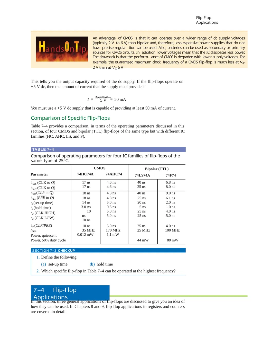
Table 7–4 provides a comparison, in terms of the operating parameters discussed in this section, of four CMOS and bipolar (TTL) flip-flops of the same type but with different IC families (HC, AHC, LS, and F). TABLE 7–4 Comparison of operating parameters for four IC families of flip-flops of the same type at 25°C. SECTION 7–3 CHECKUP Define the following:
set-up time (b) hold time
Which specific flip-flop in Table 7–4 can be operated at the highest frequency? 7–4 Flip-Flop Applications In this section, three general applications of flip-flops are discussed to give you an idea of how they can be used. In Chapters 8 and 9, flip-flop applications in registers and counters are covered in detail.<br>
slide25. Latches, Flip-Flops, and Timers
After completing this section, you should be able to ◆ Discuss the application of flip-flops in data storage Describe how flip-flops are used for frequency division
Explain how flip-flops are used in basic counter applications ◆ ◆ Parallel Data Storage
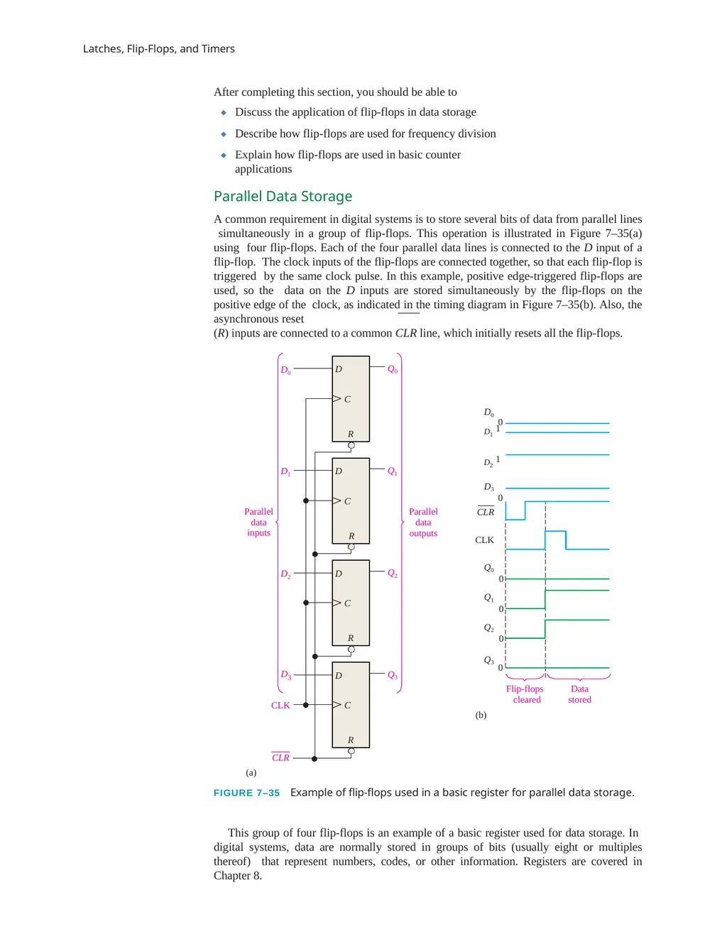
A common requirement in digital systems is to store several bits of data from parallel lines simultaneously in a group of flip-flops. This operation is illustrated in Figure 7–35(a) using four flip-flops. Each of the four parallel data lines is connected to the D input of a flip-flop. The clock inputs of the flip-flops are connected together, so that each flip-flop is triggered by the same clock pulse. In this example, positive edge-triggered flip-flops are used, so the data on the D inputs are stored simultaneously by the flip-flops on the positive edge of the clock, as indicated in the timing diagram in Figure 7–35(b). Also, the asynchronous reset
(R) inputs are connected to a common CLR line, which initially resets all the flip-flops. Q0 Parallel data inputs Q1 Q2 Q3 D0 D1 D2 D 3 CLK D0
0
D1 1
D2 1
D3
0 CLK Q3 (b) Parallel data outputs Flip-flops cleared Data stored Q0
0
Q1
0
Q2
0 D C R D C R D C R D C CLR 0 R CLR
(a)
FIGURE 7–35 Example of flip-flops used in a basic register for parallel data storage.
This group of four flip-flops is an example of a basic register used for data storage. In digital systems, data are normally stored in groups of bits (usually eight or multiples thereof) that represent numbers, codes, or other information. Registers are covered in Chapter 8.<br>
slide26. CLK
Q
(c) Q Flip-Flop Applications
Frequency Division
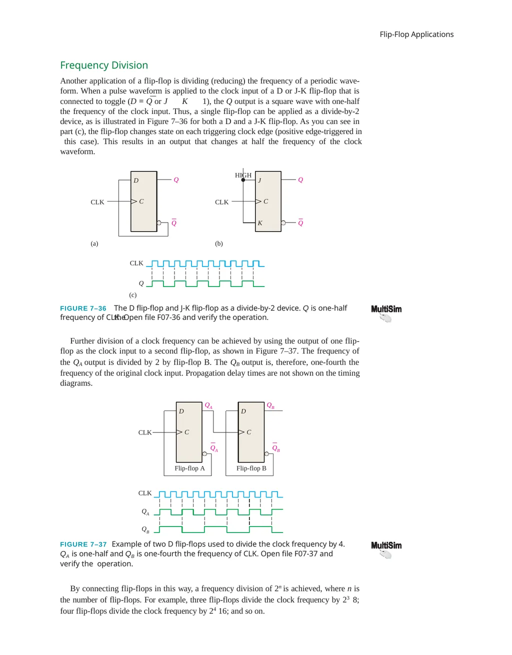
Another application of a flip-flop is dividing (reducing) the frequency of a periodic wave- form. When a pulse waveform is applied to the clock input of a D or J-K flip-flop that is connected to toggle (D = Q or J K 1), the Q output is a square wave with one-half the frequency of the clock input. Thus, a single flip-flop can be applied as a divide-by-2 device, as is illustrated in Figure 7–36 for both a D and a J-K flip-flop. As you can see in part (c), the flip-flop changes state on each triggering clock edge (positive edge-triggered in this case). This results in an output that changes at half the frequency of the clock waveform.
HIGH CLK J C K Q CLK D C (a) (b) Q Q FIGURE 7–36 The D flip-flop and J-K flip-flop as a divide-by-2 device. Q is one-half the frequency of CLK. Open file F07-36 and verify the operation.
Further division of a clock frequency can be achieved by using the output of one flip- flop as the clock input to a second flip-flop, as shown in Figure 7–37. The frequency of the QA output is divided by 2 by flip-flop B. The QB output is, therefore, one-fourth the frequency of the original clock input. Propagation delay times are not shown on the timing diagrams. CLK
QA QB
FIGURE 7–37 Example of two D flip-flops used to divide the clock frequency by 4. QA is one-half and QB is one-fourth the frequency of CLK. Open file F07-37 and verify the operation.
By connecting flip-flops in this way, a frequency division of 2n is achieved, where n is the number of flip-flops. For example, three flip-flops divide the clock frequency by 23 8; four flip-flops divide the clock frequency by 24 16; and so on. QA CLK Flip-flop A QB Flip-flop B D C D C QA QB<br>
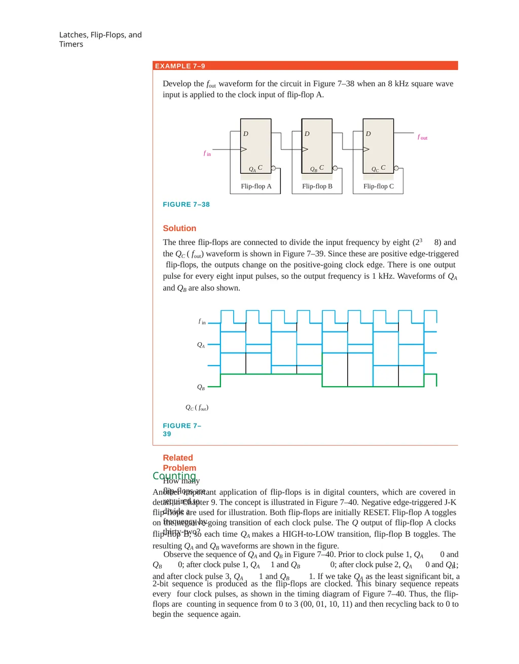
slide27. Latches, Flip-Flops, and Timers EXAMPLE 7–9 Develop the fout waveform for the circuit in Figure 7–38 when an 8 kHz square wave input is applied to the clock input of flip-flop A. D QA C Flip-flop A f in D QB C Flip-flop B D QC C Flip-flop C f out FIGURE 7–38
Solution
The three flip-flops are connected to divide the input frequency by eight (23 8) and the QC ( fout) waveform is shown in Figure 7–39. Since these are positive edge-triggered flip-flops, the outputs change on the positive-going clock edge. There is one output pulse for every eight input pulses, so the output frequency is 1 kHz. Waveforms of QA and QB are also shown. f in
QA QB
QC ( fout)
FIGURE 7–39
Related Problem
How many flip-flops are required to divide a frequency by thirty-two? Counting
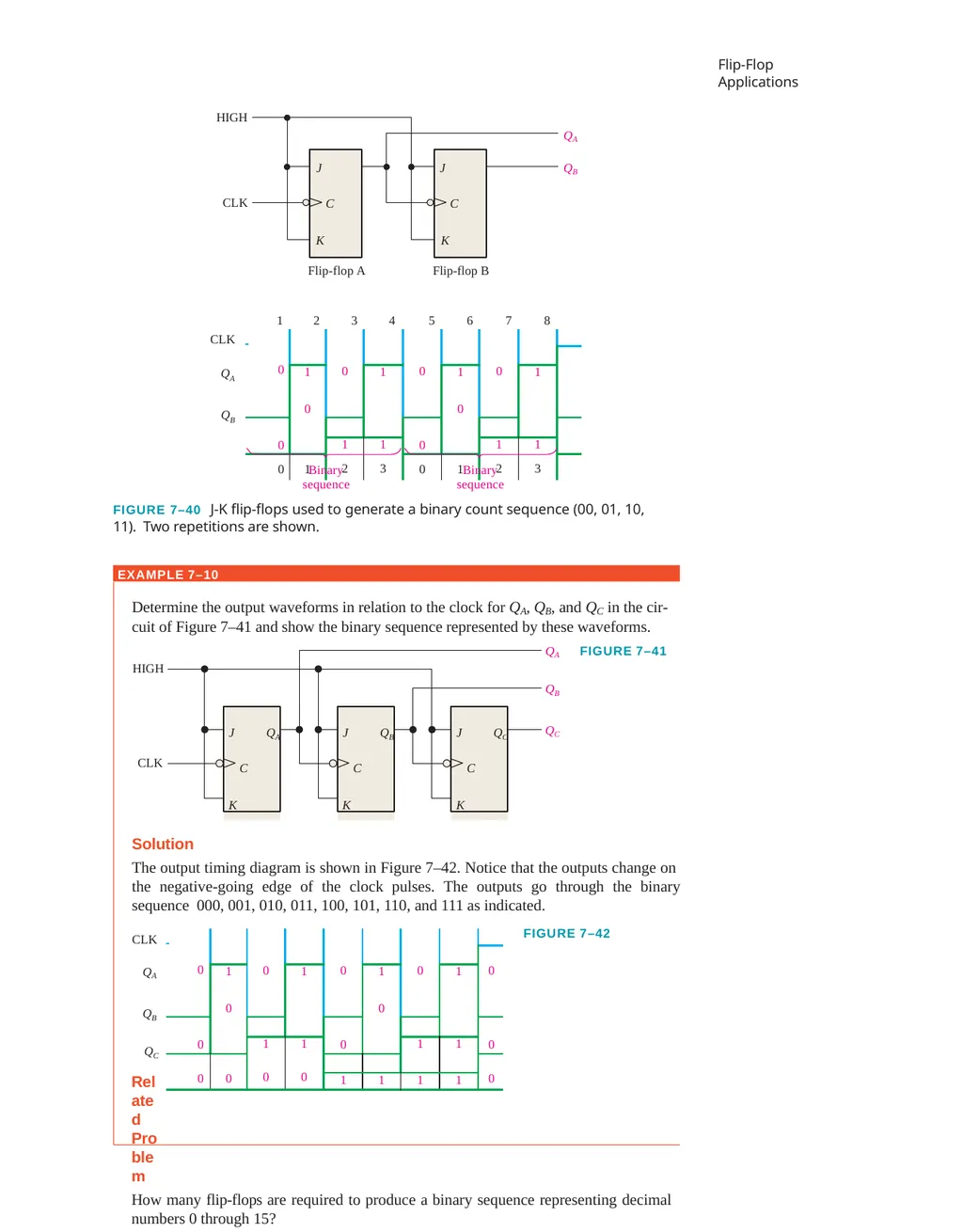
Another important application of flip-flops is in digital counters, which are covered in detail in Chapter 9. The concept is illustrated in Figure 7–40. Negative edge-triggered J-K flip-flops are used for illustration. Both flip-flops are initially RESET. Flip-flop A toggles on the negative-going transition of each clock pulse. The Q output of flip-flop A clocks flip-flop B, so each time QA makes a HIGH-to-LOW transition, flip-flop B toggles. The resulting QA and QB waveforms are shown in the figure. Observe the sequence of QA and QB in Figure 7–40. Prior to clock pulse 1, QA 0 and
1; QB 0; after clock pulse 1, QA
and after clock pulse 3, QA 1 and QB 0; after clock pulse 2, QA 0 and QB
1 and QB 1. If we take QA as the least significant bit, a 2-bit sequence is produced as the flip-flops are clocked. This binary sequence repeats every four clock pulses, as shown in the timing diagram of Figure 7–40. Thus, the flip-flops are counting in sequence from 0 to 3 (00, 01, 10, 11) and then recycling back to 0 to begin the sequence again.<br>
slide28. Flip-Flop Applications HIGH J C K CLK Flip-flop A J C K Flip-flop B QA QB 1 2 3 4 5 6 7 8 CLK
QA
QB Binary sequence Binary sequence FIGURE 7–40 J-K flip-flops used to generate a binary count sequence (00, 01, 10, 11). Two repetitions are shown. EXAMPLE 7–10 Determine the output waveforms in relation to the clock for QA, QB, and QC in the cir- cuit of Figure 7–41 and show the binary sequence represented by these waveforms. J QA
C
K J QB
C
K J QC
C
K HIGH CLK QC QB QA FIGURE 7–41 Solution
The output timing diagram is shown in Figure 7–42. Notice that the outputs change on the negative-going edge of the clock pulses. The outputs go through the binary sequence 000, 001, 010, 011, 100, 101, 110, and 111 as indicated. CLK QA
QB QC
Related Problem
How many flip-flops are required to produce a binary sequence representing decimal numbers 0 through 15? FIGURE 7–42<br>
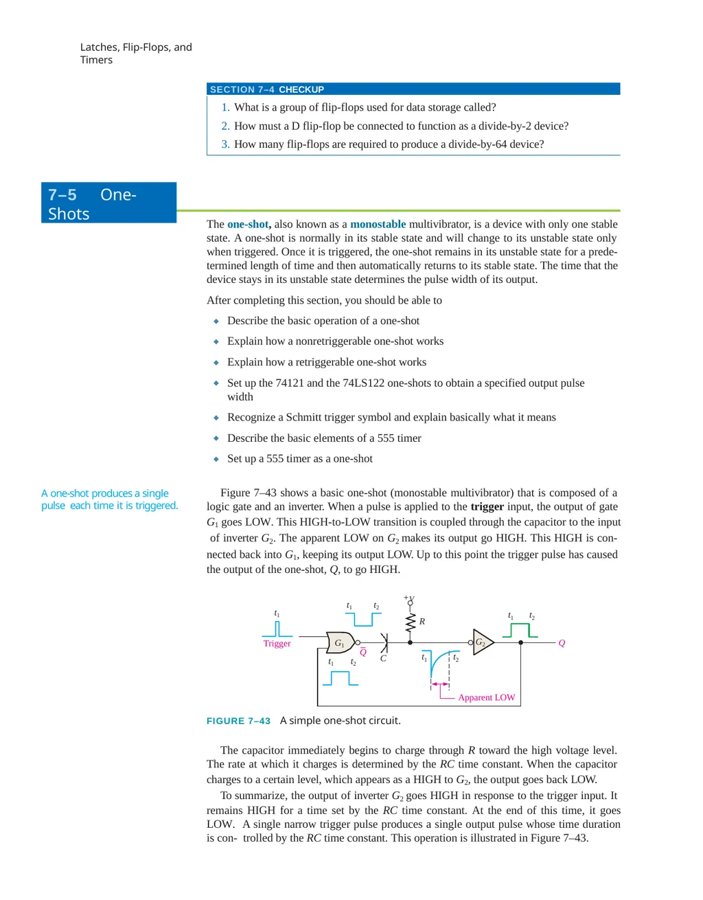
slide29. Latches, Flip-Flops, and Timers FIGURE 7–43 A simple one-shot circuit.
The capacitor immediately begins to charge through R toward the high voltage level. The rate at which it charges is determined by the RC time constant. When the capacitor charges to a certain level, which appears as a HIGH to G2, the output goes back LOW.
To summarize, the output of inverter G2 goes HIGH in response to the trigger input. It remains HIGH for a time set by the RC time constant. At the end of this time, it goes LOW. A single narrow trigger pulse produces a single output pulse whose time duration is con- trolled by the RC time constant. This operation is illustrated in Figure 7–43. SECTION 7–4 CHECKUP What is a group of flip-flops used for data storage called?
How must a D flip-flop be connected to function as a divide-by-2 device?
How many flip-flops are required to produce a divide-by-64 device? 7–5 One-Shots The one-shot, also known as a monostable multivibrator, is a device with only one stable state. A one-shot is normally in its stable state and will change to its unstable state only when triggered. Once it is triggered, the one-shot remains in its unstable state for a prede- termined length of time and then automatically returns to its stable state. The time that the device stays in its unstable state determines the pulse width of its output.
After completing this section, you should be able to ◆ Describe the basic operation of a one-shot Explain how a nonretriggerable one-shot works Explain how a retriggerable one-shot works
Set up the 74121 and the 74LS122 one-shots to obtain a specified output pulse width
Recognize a Schmitt trigger symbol and explain basically what it means Describe the basic elements of a 555 timer
Set up a 555 timer as a one-shot ◆ ◆ ◆ ◆ ◆ ◆ Figure 7–43 shows a basic one-shot (monostable multivibrator) that is composed of a logic gate and an inverter. When a pulse is applied to the trigger input, the output of gate G1 goes LOW. This HIGH-to-LOW transition is coupled through the capacitor to the input of inverter G2. The apparent LOW on G2 makes its output go HIGH. This HIGH is con- nected back into G1, keeping its output LOW. Up to this point the trigger pulse has caused the output of the one-shot, Q, to go HIGH. t1 Trigger G1 t1 t2 +V R t1 t2 G2 Q Q
t1 t2 t1 t2 Apparent LOW C A one-shot produces a single pulse each time it is triggered.<br>
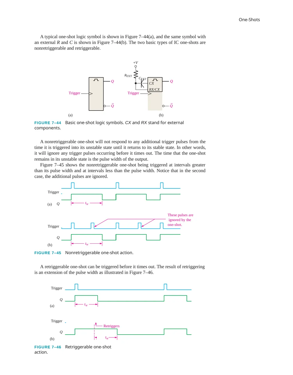
slide30. One-Shots A typical one-shot logic symbol is shown in Figure 7–44(a), and the same symbol with an external R and C is shown in Figure 7–44(b). The two basic types of IC one-shots are nonretriggerable and retriggerable.
+V Trigger Q CEXT REXT Q Q CX RX/CX Q Trigger (a) (b)
FIGURE 7–44 Basic one-shot logic symbols. CX and RX stand for external components.
A nonretriggerable one-shot will not respond to any additional trigger pulses from the time it is triggered into its unstable state until it returns to its stable state. In other words, it will ignore any trigger pulses occurring before it times out. The time that the one-shot remains in its unstable state is the pulse width of the output.
Figure 7–45 shows the nonretriggerable one-shot being triggered at intervals greater than its pulse width and at intervals less than the pulse width. Notice that in the second case, the additional pulses are ignored.
Trigger
Q Q (a) (b) tW These pulses are ignored by the one-shot. tW Trigger FIGURE 7–45 Nonretriggerable one-shot action.
A retriggerable one-shot can be triggered before it times out. The result of retriggering is an extension of the pulse width as illustrated in Figure 7–46.
Trigger
Q (a) (b) Q tW tW Retriggers Trigger FIGURE 7–46 Retriggerable one-shot action.<br>
slide31. Latches, Flip-Flops, and Timers
Nonretriggerable One-Shot
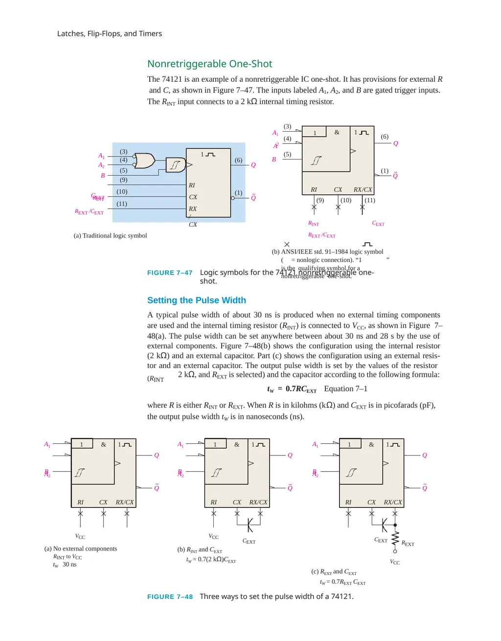
The 74121 is an example of a nonretriggerable IC one-shot. It has provisions for external R and C, as shown in Figure 7–47. The inputs labeled A1, A2, and B are gated trigger inputs. The RINT input connects to a 2 kΩ internal timing resistor. RI CX RX/CX & A 1 A2 B RINT Q Q (3) (4) (5) (9) (10) (11) REXT /CEXT C EXT (6) (1) (a) Traditional logic symbol A1 A 2 (3) B (4) (5) 1 (6)
Q Q (1) (9) (10) (11) RINT CEXT REXT /CEXT
(b) ANSI/IEEE std. 91–1984 logic symbol
( = nonlogic connection). “1 ” is the qualifying symbol for a nonretriggerable one-shot. 1 1 RI CX
RX/CX FIGURE 7–47 Logic symbols for the 74121 nonretriggerable one-shot. Setting the Pulse Width
A typical pulse width of about 30 ns is produced when no external timing components are used and the internal timing resistor (RINT) is connected to VCC, as shown in Figure 7–48(a). The pulse width can be set anywhere between about 30 ns and 28 s by the use of external components. Figure 7–48(b) shows the configuration using the internal resistor (2 kΩ) and an external capacitor. Part (c) shows the configuration using an external resis- tor and an external capacitor. The output pulse width is set by the values of the resistor (RINT 2 kΩ, and REXT is selected) and the capacitor according to the following formula: tW = 0.7RCEXT Equation 7–1
where R is either RINT or REXT. When R is in kilohms (kΩ) and CEXT is in picofarads (pF), the output pulse width tW is in nanoseconds (ns). VCC RI CX RX/CX & 1 A1 A2 B Q Q RI CX RX/CX & 1 A1 A2 B Q Q CEXT RI CX RX/CX & 1 A1 A2 B Q Q REXT VCC CEXT (a) No external components
RINT to VCC
tW 30 ns (b) RINT and CEXT
tW = 0.7(2 kΩ)CEXT (c) REXT and CEXT
tW = 0.7REXT CEXT
FIGURE 7–48 Three ways to set the pulse width of a 74121. VCC 1 1 1<br>
slide32. One-Shots The Schmitt-Trigger Symbol
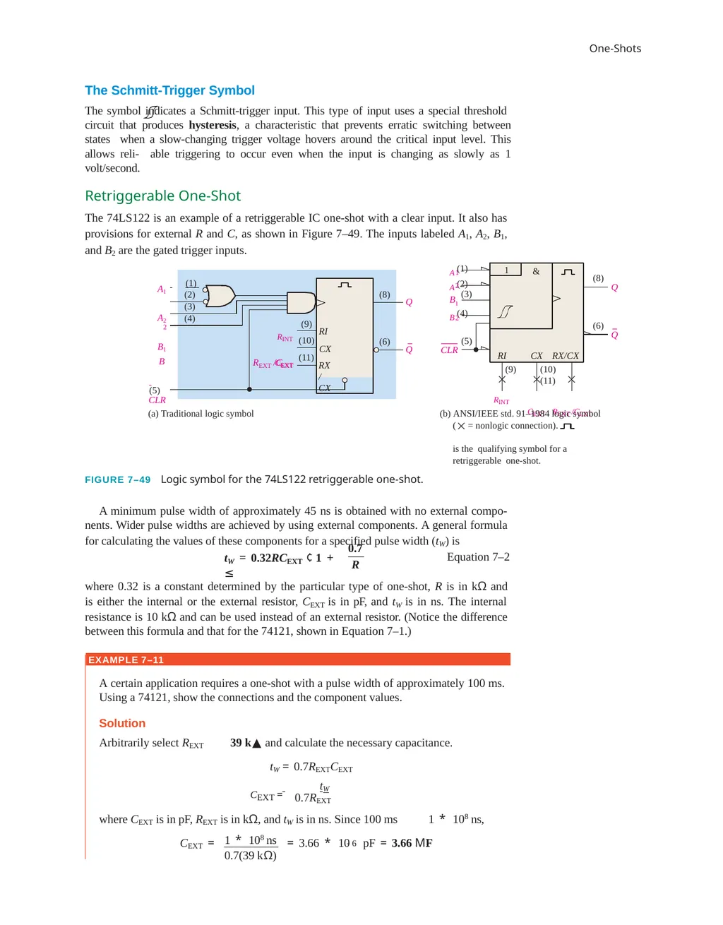
The symbol indicates a Schmitt-trigger input. This type of input uses a special threshold circuit that produces hysteresis, a characteristic that prevents erratic switching between states when a slow-changing trigger voltage hovers around the critical input level. This allows reli- able triggering to occur even when the input is changing as slowly as 1 volt/second.
Retriggerable One-Shot
The 74LS122 is an example of a retriggerable IC one-shot with a clear input. It also has provisions for external R and C, as shown in Figure 7–49. The inputs labeled A1, A2, B1, and B2 are the gated trigger inputs. RI & 1 Q Q (1) (2) (3) (9)
(10)
(11) R /C EXT EXT RINT CEXT (8) (6) RI CX
RX/CX (a) Traditional logic symbol 1 A (1) A (2) 2
(3) (8)
Q (6)
Q (9) RINT CX RX/CX
(10) (11)
CEXT REXT /CEXT (b) ANSI/IEEE std. 91–1984 logic symbol ( = nonlogic connection). is the qualifying symbol for a retriggerable one-shot.
FIGURE 7–49 Logic symbol for the 74LS122 retriggerable one-shot.
A minimum pulse width of approximately 45 ns is obtained with no external compo- nents. Wider pulse widths are achieved by using external components. A general formula for calculating the values of these components for a specified pulse width (tW) is (4) A1 A2 B1 B 2 (5)
CLR B1 B (4) 2 (5)
CLR 0.7 R tW = 0.32RCEXT ¢ 1 + ≤ Equation 7–2 where 0.32 is a constant determined by the particular type of one-shot, R is in kΩ and is either the internal or the external resistor, CEXT is in pF, and tW is in ns. The internal resistance is 10 kΩ and can be used instead of an external resistor. (Notice the difference between this formula and that for the 74121, shown in Equation 7–1.) EXAMPLE 7–11 CEXT = A certain application requires a one-shot with a pulse width of approximately 100 ms. Using a 74121, show the connections and the component values.
Solution
Arbitrarily select REXT 39 k▲ and calculate the necessary capacitance.
tW = 0.7REXTCEXT
tW 0.7REXT where CEXT is in pF, REXT is in kΩ, and tW is in ns. Since 100 ms 1 * 108 ns, 1 * 108 ns -6 CEXT = = 3.66 * 10 pF = 3.66 MF
0.7(39 kΩ)<br>
slide33. Latches, Flip-Flops, and Timers
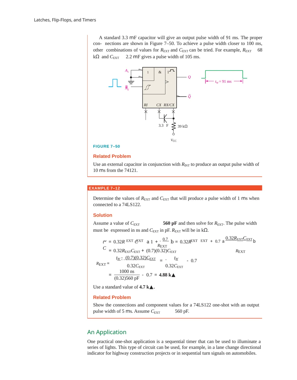
A standard 3.3 mF capacitor will give an output pulse width of 91 ms. The proper con- nections are shown in Figure 7–50. To achieve a pulse width closer to 100 ms, other combinations of values for REXT and CEXT can be tried. For example, REXT 68 kΩ and CEXT 2.2 mF gives a pulse width of 105 ms. RI CX RX/CX tW = 91 ms A1 A2 B Q Q VCC 39 kΩ 3.3 F 1 & 1 FIGURE 7–50
Related Problem
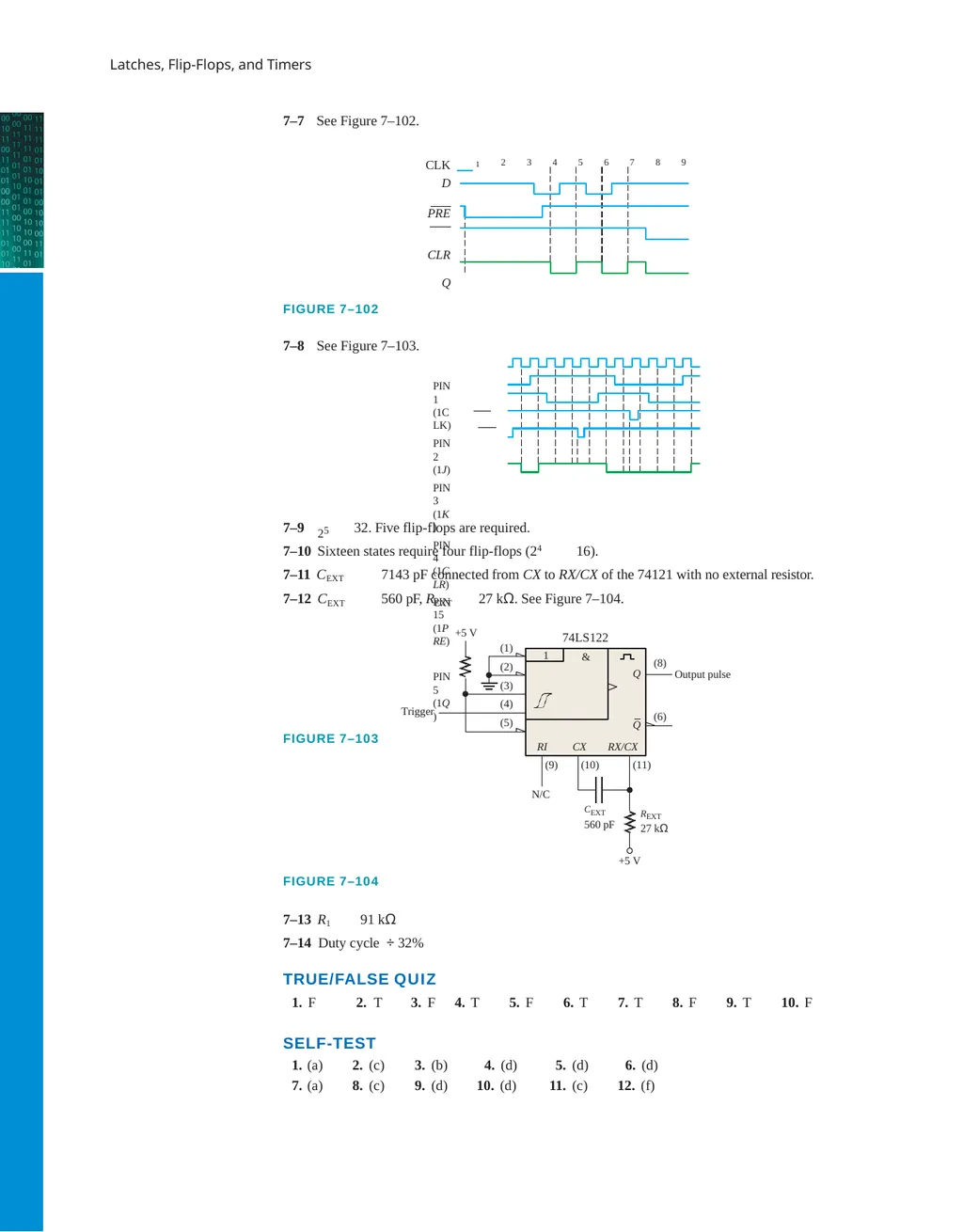
Use an external capacitor in conjunction with RINT to produce an output pulse width of 10 ms from the 74121. EXAMPLE 7–12 Determine the values of REXT and CEXT that will produce a pulse width of 1 ms when connected to a 74LS122.
Solution
Assume a value of CEXT 560 pF and then solve for REXT. The pulse width must be expressed in ns and CEXT in pF. REXT will be in kΩ. w EXT EXT REXT t = 0.32R C a 1 + 0.7 b = 0.32R C EXT EXT + 0.7 a 0.32REXTCEXT b
REXT = 0.32REXTCEXT + (0.7)(0.32)CEXT REXT = tW - (0.7)(0.32)CEXT
0.32CEXT = tW
0.32CEXT - 0.7 = 1000 ns (0.32)560 pF - 0.7 = 4.88 k▲ Use a standard value of 4.7 k▲.
Related Problem
Show the connections and component values for a 74LS122 one-shot with an output pulse width of 5 ms. Assume CEXT 560 pF.
An Application
One practical one-shot application is a sequential timer that can be used to illuminate a series of lights. This type of circuit can be used, for example, in a lane change directional indicator for highway construction projects or in sequential turn signals on automobiles.<br>
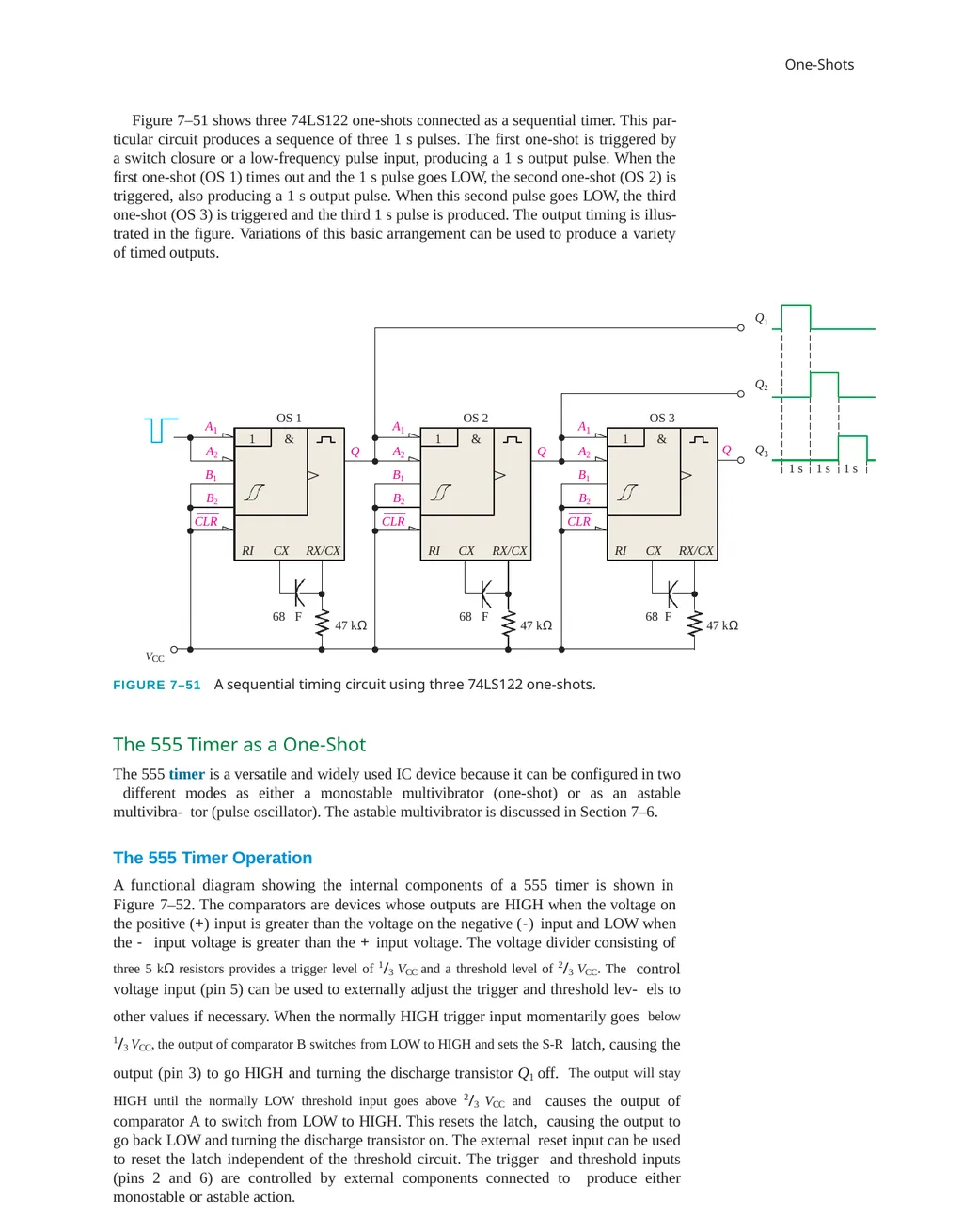
slide34. One-Shots Figure 7–51 shows three 74LS122 one-shots connected as a sequential timer. This par- ticular circuit produces a sequence of three 1 s pulses. The first one-shot is triggered by a switch closure or a low-frequency pulse input, producing a 1 s output pulse. When the first one-shot (OS 1) times out and the 1 s pulse goes LOW, the second one-shot (OS 2) is triggered, also producing a 1 s output pulse. When this second pulse goes LOW, the third one-shot (OS 3) is triggered and the third 1 s pulse is produced. The output timing is illus- trated in the figure. Variations of this basic arrangement can be used to produce a variety of timed outputs. 68 F 47 kΩ RI CX RX/CX & OS 3 47 kΩ RI CX RX/CX & RI CX RX/CX & Q OS 2 OS 1 Q1 Q2 Q3 1 s 1 s 1 s Q Q A 1 A2 B1 B2 CLR A 1 A2 B1 B2 CLR A 1 A2 B1 B2 CLR 47 kΩ 68 F 68 F 1 1 1 VCC
FIGURE 7–51 A sequential timing circuit using three 74LS122 one-shots.
The 555 Timer as a One-Shot
The 555 timer is a versatile and widely used IC device because it can be configured in two different modes as either a monostable multivibrator (one-shot) or as an astable multivibra- tor (pulse oscillator). The astable multivibrator is discussed in Section 7–6.
The 555 Timer Operation
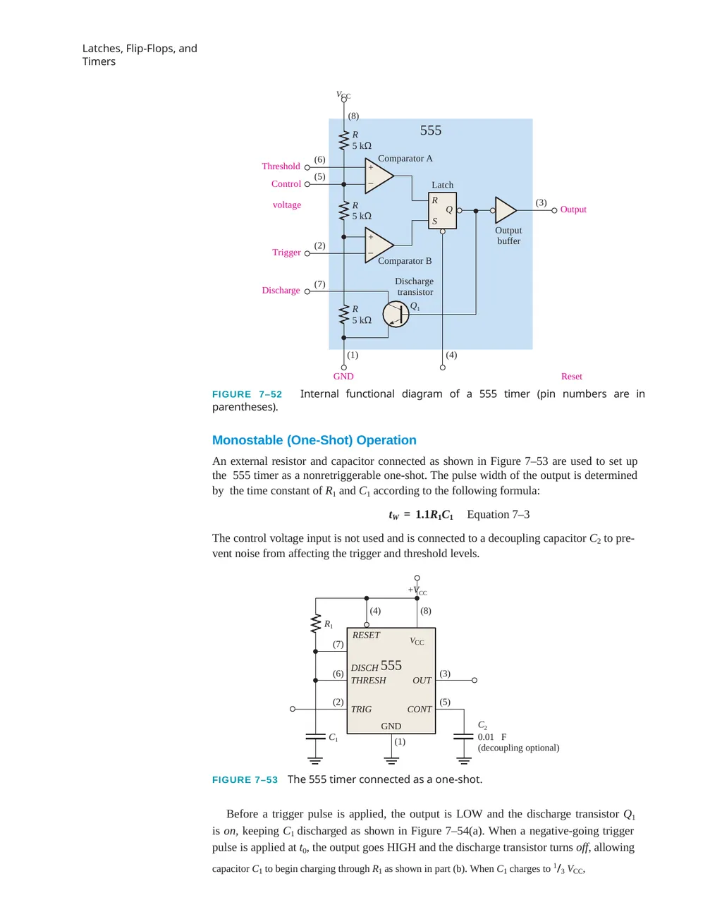
A functional diagram showing the internal components of a 555 timer is shown in Figure 7–52. The comparators are devices whose outputs are HIGH when the voltage on the positive (+) input is greater than the voltage on the negative (-) input and LOW when the - input voltage is greater than the + input voltage. The voltage divider consisting of three 5 kΩ resistors provides a trigger level of 1/3 VCC and a threshold level of 2/3 VCC. The control voltage input (pin 5) can be used to externally adjust the trigger and threshold lev- els to other values if necessary. When the normally HIGH trigger input momentarily goes below 1/3 VCC, the output of comparator B switches from LOW to HIGH and sets the S-R latch, causing the output (pin 3) to go HIGH and turning the discharge transistor Q1 off. The output will stay HIGH until the normally LOW threshold input goes above 2/3 VCC and causes the output of comparator A to switch from LOW to HIGH. This resets the latch, causing the output to go back LOW and turning the discharge transistor on. The external reset input can be used to reset the latch independent of the threshold circuit. The trigger and threshold inputs (pins 2 and 6) are controlled by external components connected to produce either monostable or astable action.<br>
slide35. Latches, Flip-Flops, and Timers R
5 kΩ Output + – + – Output buffer Latch Comparator B VCC
(8) Comparator A R
5 kΩ R
5 kΩ Discharge Trigger Threshold
Control voltage (6) (5) (2) (7) (1) (4) (3) Discharge transistor
Q1 R S Q 555 GND Reset
FIGURE 7–52 Internal functional diagram of a 555 timer (pin numbers are in parentheses).
Monostable (One-Shot) Operation
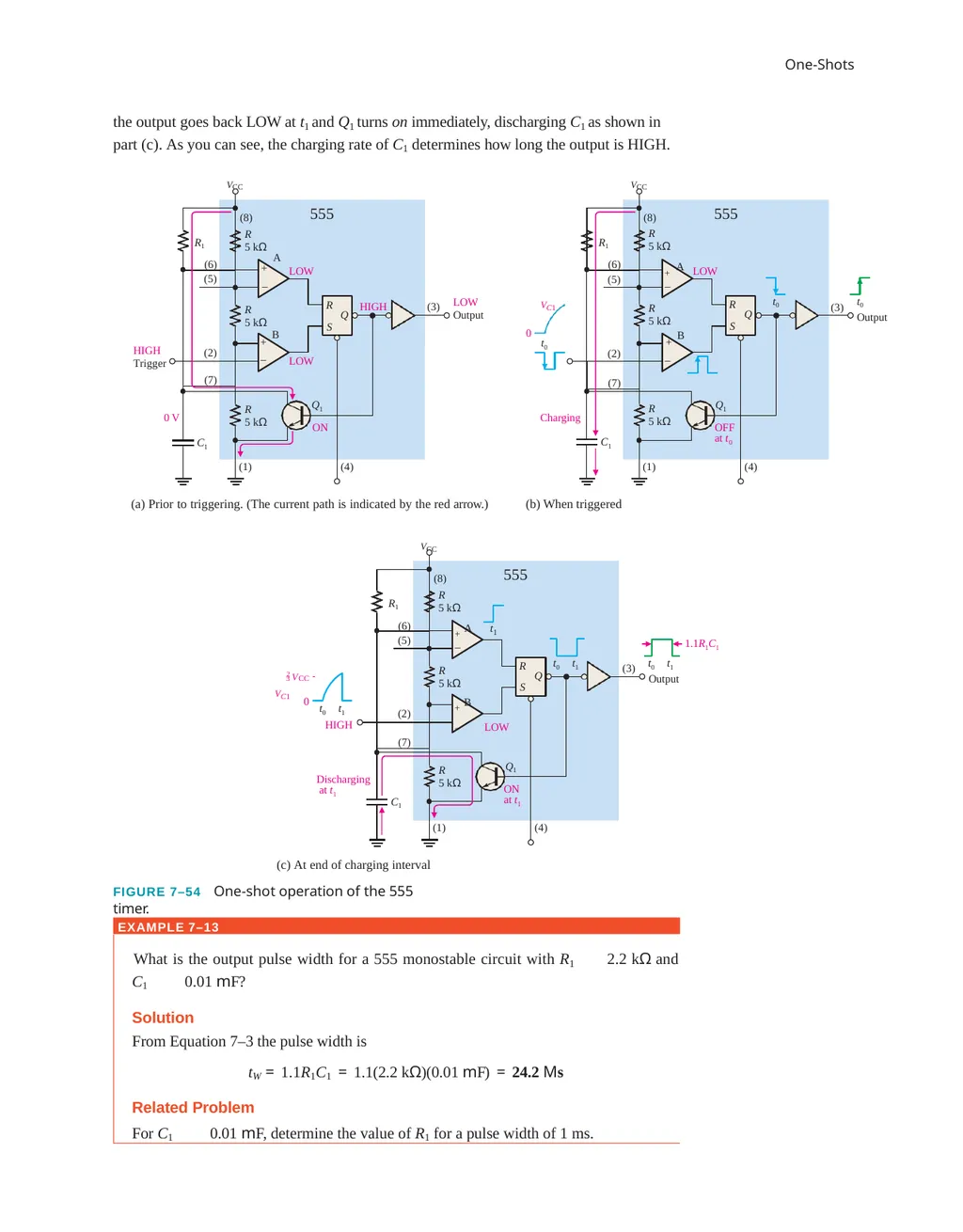
An external resistor and capacitor connected as shown in Figure 7–53 are used to set up the 555 timer as a nonretriggerable one-shot. The pulse width of the output is determined by the time constant of R1 and C1 according to the following formula:
tW = 1.1R1C1 Equation 7–3
The control voltage input is not used and is connected to a decoupling capacitor C2 to pre- vent noise from affecting the trigger and threshold levels.
+VCC VCC RESET DISCH 555
THRESH TRIG (7) (6) (2) (3) (5) R1 (4) (8) GND (1) OUT CONT C1 C2
0.01 F
(decoupling optional) FIGURE 7–53 The 555 timer connected as a one-shot.
Before a trigger pulse is applied, the output is LOW and the discharge transistor Q1 is on, keeping C1 discharged as shown in Figure 7–54(a). When a negative-going trigger pulse is applied at t0, the output goes HIGH and the discharge transistor turns off, allowing capacitor C1 to begin charging through R1 as shown in part (b). When C1 charges to 1/3 VCC,<br>
slide36. One-Shots the output goes back LOW at t1 and Q1 turns on immediately, discharging C1 as shown in part (c). As you can see, the charging rate of C1 determines how long the output is HIGH. VCC LOW
Output R S Q – – B (8)
R
5 kΩ
A
+ R
5 kΩ
+ R
5 kΩ HIGH
Trigger (5) (2) (7) (1) (4) (3) Q1 LOW LOW HIGH ON C1 R1
(6) 0 V (a) Prior to triggering. (The current path is indicated by the red arrow.) R
S Q – – B (8)
R
5 kΩ
+ A R
5 kΩ
+ R
5 kΩ (5) (2) (7) (1) (4) (3) Q1 LOW t0 OFF
at t0 Charging (b) When triggered VCC R S Q – (8)
R
5 kΩ
+ A R
5 kΩ
+ B R
5 kΩ (5) (2) (7) (1) (4) (3) Q1 – LOW R1
(6) Discharging at t1 (c) At end of charging interval
FIGURE 7–54 One-shot operation of the 555 timer. VC1 0 1.1R1C1 2 V – CC 0 3
VC1 555 555 555 C1 t0 t1
Output t0 t1
HIGH C1 t0
Output t0 VCC R1
(6) t0 t1 t 1 ON
at t1 EXAMPLE 7–13 What is the output pulse width for a 555 monostable circuit with R1 2.2 kΩ and
C1 0.01 mF?
Solution
From Equation 7–3 the pulse width is
tW = 1.1R1C1 = 1.1(2.2 kΩ)(0.01 mF) = 24.2 Ms
Related Problem
For C1 0.01 mF, determine the value of R1 for a pulse width of 1 ms.<br>
slide37. Latches, Flip-Flops, and Timers
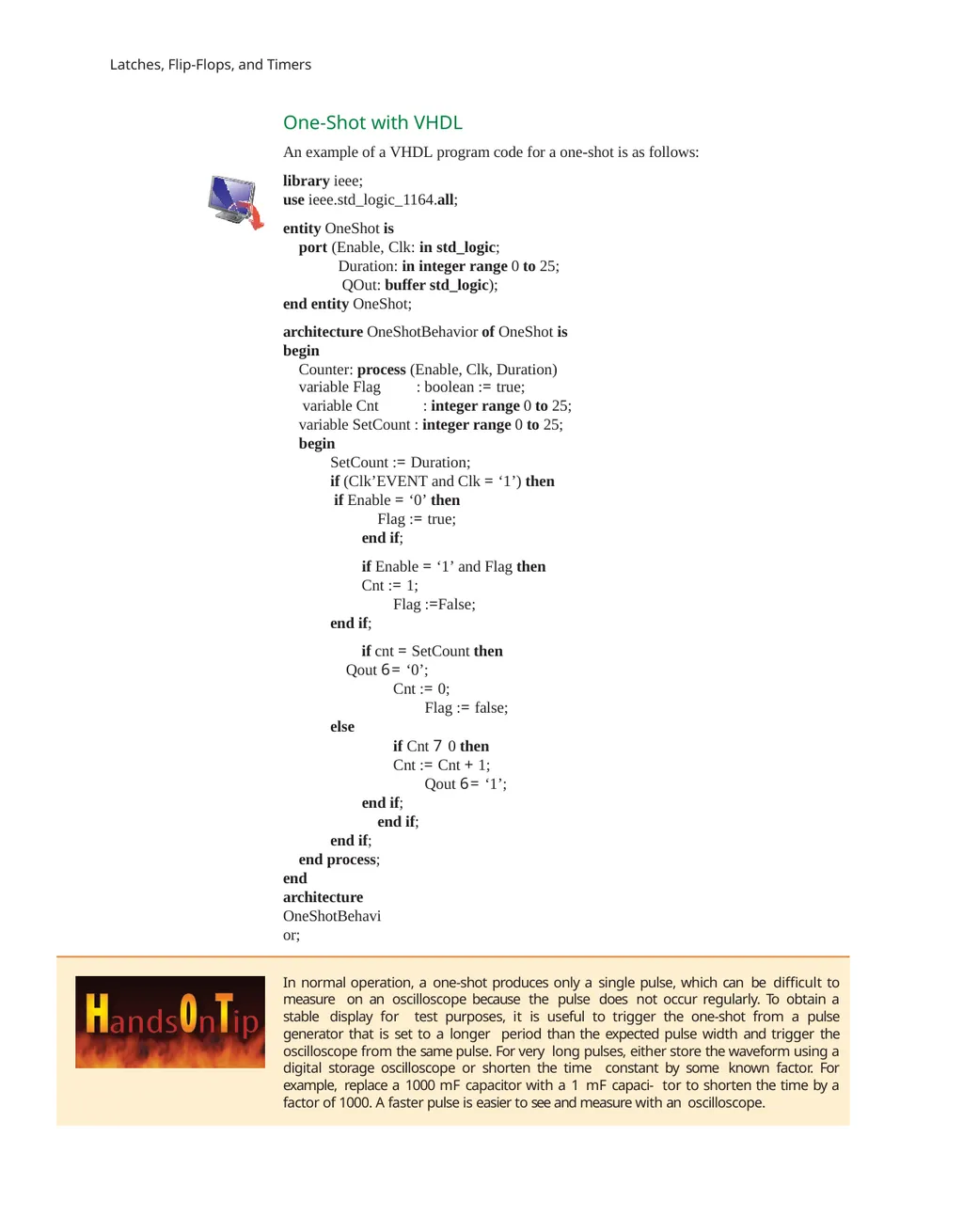
One-Shot with VHDL
An example of a VHDL program code for a one-shot is as follows:
library ieee;
use ieee.std_logic_1164.all;
entity OneShot is
port (Enable, Clk: in std_logic; Duration: in integer range 0 to 25; QOut: buffer std_logic);
end entity OneShot;
architecture OneShotBehavior of OneShot is begin
Counter: process (Enable, Clk, Duration) variable Flag variable Cnt : boolean := true;
: integer range 0 to 25; variable SetCount : integer range 0 to 25;
begin
SetCount := Duration;
if (Clk’EVENT and Clk = ‘1’) then if Enable = ‘0’ then
Flag := true;
end if;
if Enable = ‘1’ and Flag then
Cnt := 1;
Flag :=False;
end if;
if cnt = SetCount then
Qout 6= ‘0’;
Cnt := 0;
Flag := false;
else
if Cnt 7 0 then
Cnt := Cnt + 1;
Qout 6= ‘1’;
end if;
end if;
end if; end process;
end architecture OneShotBehavior; In normal operation, a one-shot produces only a single pulse, which can be difficult to measure on an oscilloscope because the pulse does not occur regularly. To obtain a stable display for test purposes, it is useful to trigger the one-shot from a pulse generator that is set to a longer period than the expected pulse width and trigger the oscilloscope from the same pulse. For very long pulses, either store the waveform using a digital storage oscilloscope or shorten the time constant by some known factor. For example, replace a 1000 mF capacitor with a 1 mF capaci- tor to shorten the time by a factor of 1000. A faster pulse is easier to see and measure with an oscilloscope.<br>
slide38. The Astable Multivibrator The 555 Timer as an Astable Multivibrator
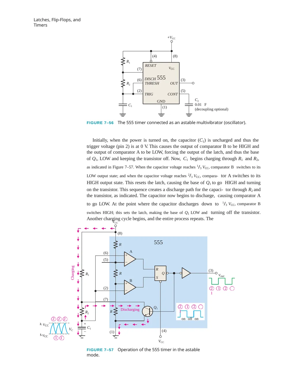
A 555 timer connected to operate as an astable multivibrator is shown in Figure 7–56. Notice that the threshold input (THRESH) is now connected to the trigger input (TRIG). 1 2 1 The external components R , R , and C form the timing network that sets the frequency of oscillation. The 0.01 mF capacitor, C2, connected to the control (CONT) input is strictly for decoupling and has no effect on the operation; in some cases it can be left off. SECTION 7–5 CHECKUP Describe the difference between a nonretriggerable and a retriggerable one-shot.
How is the output pulse width set in most IC one-shots?
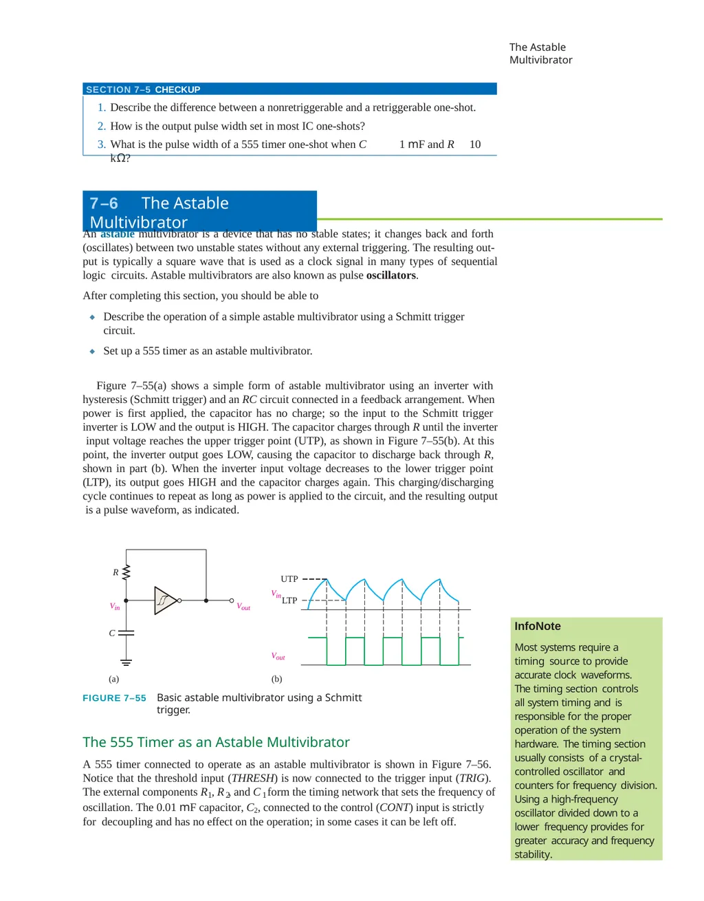
What is the pulse width of a 555 timer one-shot when C 1 mF and R 10 kΩ? 7–6 The Astable Multivibrator An astable multivibrator is a device that has no stable states; it changes back and forth (oscillates) between two unstable states without any external triggering. The resulting out- put is typically a square wave that is used as a clock signal in many types of sequential logic circuits. Astable multivibrators are also known as pulse oscillators.
After completing this section, you should be able to ◆ Describe the operation of a simple astable multivibrator using a Schmitt trigger circuit. ◆ Set up a 555 timer as an astable multivibrator. Figure 7–55(a) shows a simple form of astable multivibrator using an inverter with hysteresis (Schmitt trigger) and an RC circuit connected in a feedback arrangement. When power is first applied, the capacitor has no charge; so the input to the Schmitt trigger inverter is LOW and the output is HIGH. The capacitor charges through R until the inverter input voltage reaches the upper trigger point (UTP), as shown in Figure 7–55(b). At this point, the inverter output goes LOW, causing the capacitor to discharge back through R, shown in part (b). When the inverter input voltage decreases to the lower trigger point (LTP), its output goes HIGH and the capacitor charges again. This charging/discharging cycle continues to repeat as long as power is applied to the circuit, and the resulting output is a pulse waveform, as indicated. (a) (b) UTP LTP Vout Vin R C Vout Vin FIGURE 7–55 Basic astable multivibrator using a Schmitt trigger. InfoNote
Most systems require a timing source to provide accurate clock waveforms. The timing section controls all system timing and is responsible for the proper
operation of the system hardware. The timing section usually consists of a crystal-controlled oscillator and counters for frequency division. Using a high-frequency oscillator divided down to a lower frequency provides for greater accuracy and frequency stability.<br>
slide39. Latches, Flip-Flops, and Timers FIGURE 7–56 The 555 timer connected as an astable multivibrator (oscillator).
Initially, when the power is turned on, the capacitor (C1) is uncharged and thus the trigger voltage (pin 2) is at 0 V. This causes the output of comparator B to be HIGH and the output of comparator A to be LOW, forcing the output of the latch, and thus the base of Q1, LOW and keeping the transistor off. Now, C1 begins charging through R1 and R2, as indicated in Figure 7–57. When the capacitor voltage reaches 1/3 VCC, comparator B switches to its LOW output state; and when the capacitor voltage reaches 2/3 VCC, compara- tor A switches to its HIGH output state. This resets the latch, causing the base of Q1 to go HIGH and turning on the transistor. This sequence creates a discharge path for the capaci- tor through R2 and the transistor, as indicated. The capacitor now begins to discharge, causing comparator A to go LOW. At the point where the capacitor discharges down to 1/3 VCC, comparator B switches HIGH; this sets the latch, making the base of Q1 LOW and turning off the transistor. Another charging cycle begins, and the entire process repeats. The C2
0.01 F
(decoupling optional) VCC RESET DISCH (7) (6) (2) (3) (5) C1 (4) (8) GND (1) 555
THRESH OUT TRIG CONT +VCC R1 R2 R R S Q – + – B VCC
(8) A
+ R (6) (5) (2) (7) (1) (4) (3) Q1 Discharging Vout 2– VCC 3 R 2 1 2 1
on off on 2 1 2 1 R1 R2 – VC Charging 555 1–VCC 3 2 2 2 1 1 +
C1 VCC
FIGURE 7–57 Operation of the 555 timer in the astable mode.<br>
slide40. The Astable Multivibrator
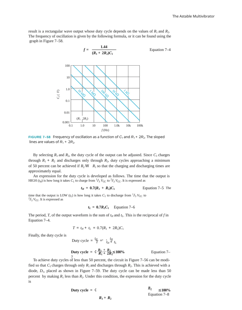
result is a rectangular wave output whose duty cycle depends on the values of R1 and R2. The frequency of oscillation is given by the following formula, or it can be found using the graph in Figure 7–58. f = 1.44 (R1 + 2R2)C1 Equation 7–4 C1 ( F) 10 MΩ 1 MΩ 100 kΩ 10 kΩ 1 kΩ 0.001 0.1 1.0 10 100
f (Hz) 100
10
1.0
0.1
0.01
(R1 2R2) 1.0k 10k 100k FIGURE 7–58 Frequency of oscillation as a function of C1 and R1 + 2R2. The sloped lines are values of R1 + 2R2.
By selecting R1 and R2, the duty cycle of the output can be adjusted. Since C1 charges through R1 + R2 and discharges only through R2, duty cycles approaching a minimum of 50 percent can be achieved if R2 W R1 so that the charging and discharging times are approximately equal.
An expression for the duty cycle is developed as follows. The time that the output is HIGH (tH) is how long it takes C1 to charge from 1/3 VCC to 2/3 VCC. It is expressed as
tH = 0.7(R1 + R2)C1 Equation 7–5 The time that the output is LOW (tL) is how long it takes C1 to discharge from 1/3 VCC to
2/3 VCC. It is expressed as
tL = 0.7R2C1 Equation 7–6
The period, T, of the output waveform is the sum of tH and tL. This is the reciprocal of f in Equation 7–4.
T = tH + tL = 0.7(R1 + 2R2)C1
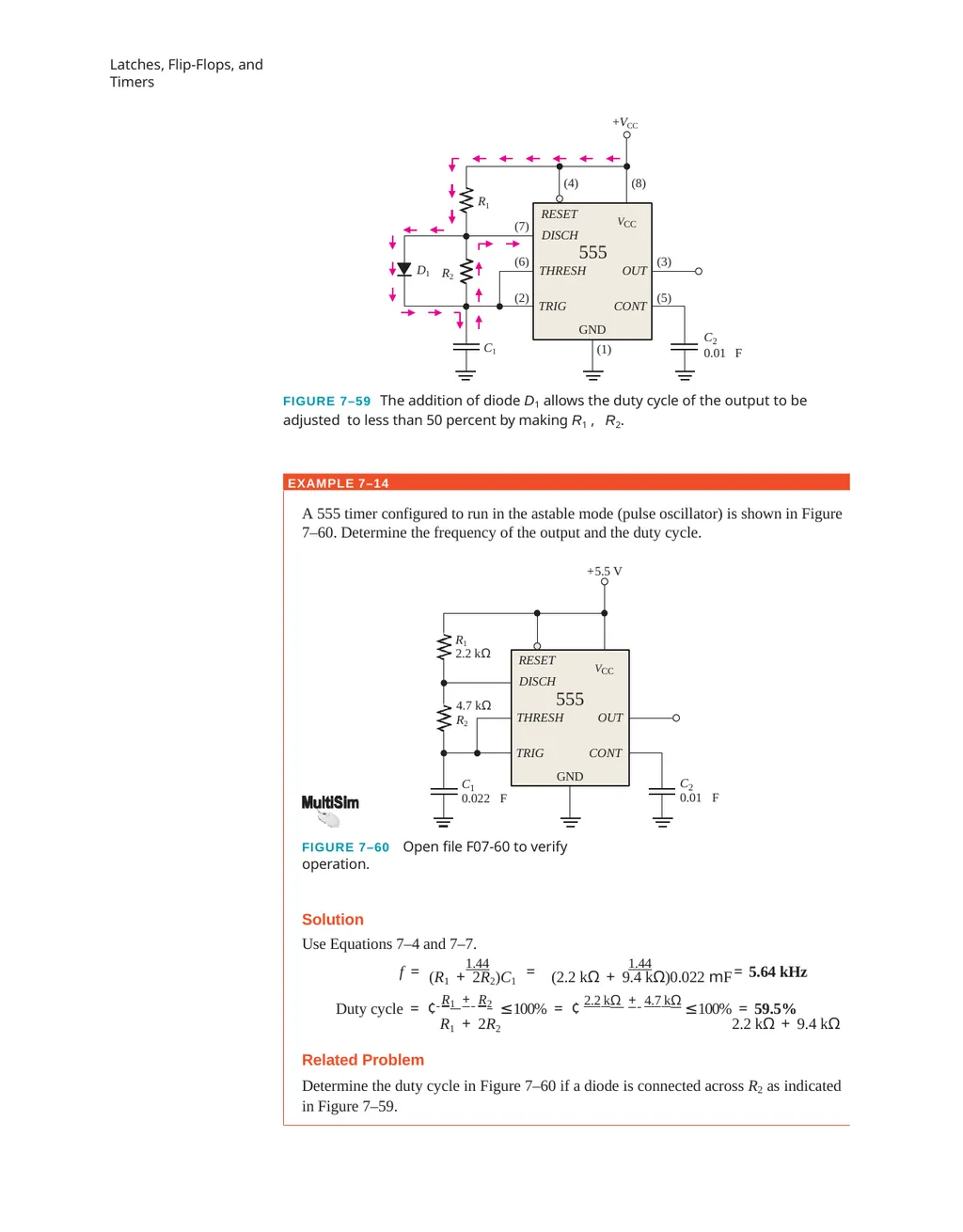
Finally, the duty cycle is Duty cycle = tH = tH T tH + tL R1 + 2R2 Duty cycle = ¢ R1 + R2 ≤100% Equation 7–7 To achieve duty cycles of less than 50 percent, the circuit in Figure 7–56 can be modi- fied so that C1 charges through only R1 and discharges through R2. This is achieved with a diode, D1, placed as shown in Figure 7–59. The duty cycle can be made less than 50 percent by making R1 less than R2. Under this condition, the expression for the duty cycle is
Duty cycle = ¢ R1 ≤100% Equation 7–8
R1 + R2<br>
slide41. Latches, Flip-Flops, and Timers C 2 0.01 F VCC RESET DISCH (7) (6) (2) (3) (5) +VCC R1 (4) (8) GND (1) 555
THRESH OUT TRIG CONT R2 D1 C1 FIGURE 7–59 The addition of diode D1 allows the duty cycle of the output to be adjusted to less than 50 percent by making R1 , R2. EXAMPLE 7–14 C 2 VCC RESET DISCH A 555 timer configured to run in the astable mode (pulse oscillator) is shown in Figure 7–60. Determine the frequency of the output and the duty cycle.
+5.5 V R1 2.2 kΩ GND 555
THRESH OUT TRIG CONT R2 C 1 4.7 kΩ 0.01 F 0.022 F FIGURE 7–60 Open file F07-60 to verify operation.
Solution
Use Equations 7–4 and 7–7. (R1 + 2R2)C1 (2.2 kΩ + 9.4 kΩ)0.022 mF f = 1.44 = 1.44 = 5.64 kHz Duty cycle = ¢ R1 + R2 ≤100% = ¢ 2.2 kΩ + 4.7 kΩ ≤100% = 59.5%
R1 + 2R2 2.2 kΩ + 9.4 kΩ
Related Problem
Determine the duty cycle in Figure 7–60 if a diode is connected across R2 as indicated in Figure 7–59.<br>
slide42. Troubleshooting SECTION 7–6 CHECKUP Explain the difference in operation between an astable multivibrator and a monosta- ble multivibrator.
For a certain astable multivibrator, tH 15 ms and T 20 ms. What is the duty cycle of the output? 7–7 Troubleshooting It is standard practice to test a new circuit design to be sure that it is operating as specified. New fixed-function designs are “breadboarded” and tested before the design is finalized. The term breadboard refers to a method of temporarily hooking up a circuit so that its operation can be verified and any design flaws worked out before a prototype unit is built.
After completing this section, you should be able to ◆ Describe how the timing of a circuit can produce erroneous glitches
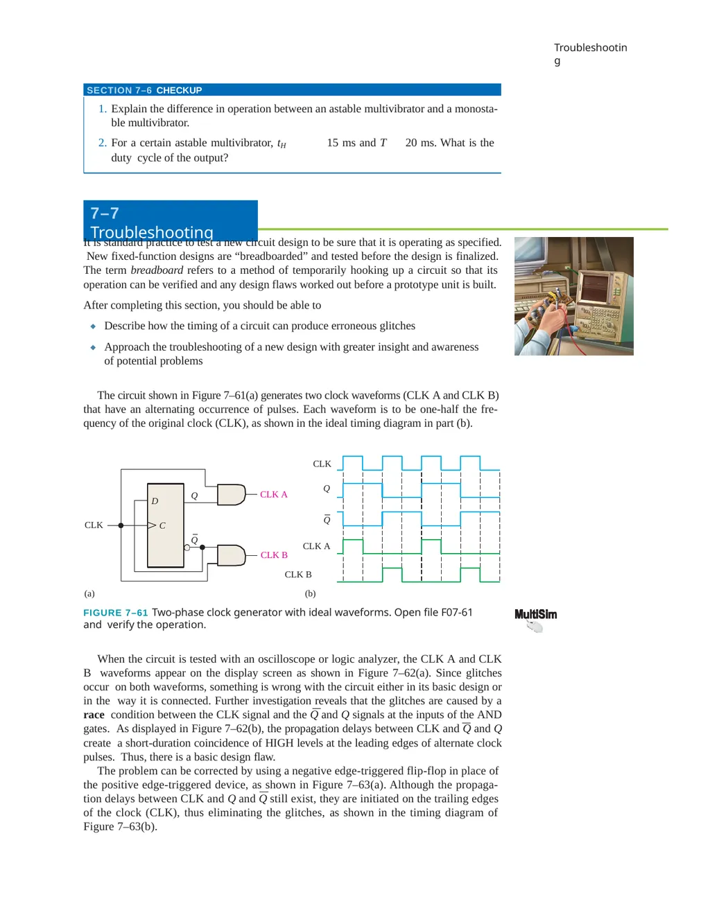
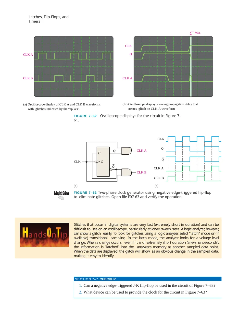
Approach the troubleshooting of a new design with greater insight and awareness of potential problems ◆ CLK CLK A CLK A The circuit shown in Figure 7–61(a) generates two clock waveforms (CLK A and CLK B) that have an alternating occurrence of pulses. Each waveform is to be one-half the fre- quency of the original clock (CLK), as shown in the ideal timing diagram in part (b).
CLK Q D C Q Q Q CLK B
CLK B
(a) (b)
FIGURE 7–61 Two-phase clock generator with ideal waveforms. Open file F07-61 and verify the operation.
When the circuit is tested with an oscilloscope or logic analyzer, the CLK A and CLK B waveforms appear on the display screen as shown in Figure 7–62(a). Since glitches occur on both waveforms, something is wrong with the circuit either in its basic design or in the way it is connected. Further investigation reveals that the glitches are caused by a race condition between the CLK signal and the Q and Q signals at the inputs of the AND gates. As displayed in Figure 7–62(b), the propagation delays between CLK and Q and Q create a short-duration coincidence of HIGH levels at the leading edges of alternate clock pulses. Thus, there is a basic design flaw.
The problem can be corrected by using a negative edge-triggered flip-flop in place of the positive edge-triggered device, as shown in Figure 7–63(a). Although the propaga- tion delays between CLK and Q and Q still exist, they are initiated on the trailing edges of the clock (CLK), thus eliminating the glitches, as shown in the timing diagram of Figure 7–63(b).<br>
slide43. Latches, Flip-Flops, and Timers CLK A CLK B (a) Oscilloscope display of CLK A and CLK B waveforms with glitches indicated by the “spikes”. CLK Q CLK A ( b) Oscilloscope display showing propagation delay that creates glitch on CLK A waveform tPHL FIGURE 7–62 Oscilloscope displays for the circuit in Figure 7–61. Q CLK CLK A CLK A CLK B
CLK B CLK Q Q Q D C (a) (b)
FIGURE 7–63 Two-phase clock generator using negative edge-triggered flip-flop to eliminate glitches. Open file F07-63 and verify the operation. SECTION 7–7 CHECKUP Can a negative edge-triggered J-K flip-flop be used in the circuit of Figure 7–63?
What device can be used to provide the clock for the circuit in Figure 7–63? Glitches that occur in digital systems are very fast (extremely short in duration) and can be difficult to see on an oscilloscope, particularly at lower sweep rates. A logic analyzer, however, can show a glitch easily. To look for glitches using a logic analyzer, select “latch” mode or (if available) transitional sampling. In the latch mode, the analyzer looks for a voltage level change. When a change occurs, even if it is of extremely short duration (a few nanoseconds), the information is “latched” into the analyzer’s memory as another sampled data point. When the data are displayed, the glitch will show as an obvious change in the sampled data, making it easy to identify.<br>
slide44. Applied Logic Applied Logic
Traffic Signal Controller: Part 2 The combinational logic unit of the traffic signal controller was completed in Chapter 6. Now, the timing circuits and sequential logic are developed. Recall that the timing circuits produce a 25 s time interval for the red and green lights and a 4 s interval for the yellow caution light. These outputs will be used by the sequential logic. The block diagram of the complete traffic signal controller is shown in Figure 7–64. Traffic light interface unit Sequential logic Long trigger Short trigger G0
G1 Short Long timer timer Vehicle sensor input
System clock Timing circuits Traffic signal control logic
Combinational logic MR MY
MG SR SY
SG FIGURE 7–64 Block diagram of the traffic signal controller. Timing Circuits
The timing circuits unit of the traffic signal controller consists of a 25 s timer and a 4 s timer and a clock generator. One way to implement this unit is with two 555 timers configured as one-shots and one 555 timer configured as an astable multivibrator (oscil- lator), as discussed earlier in this chapter. Component values are calculated based on the formulas given.
Another way to implement the timing circuits is shown in Figure 7–65. An exter- nal 24 MHz system clock (arbitrary value) is divided down to an accurate 1 Hz clock by the frequency divider. The 1 Hz clock is then used to establish the 25 s and the 4 s intervals by counting the 1 Hz pulses. This approach lends itself better to a VHDL description.<br>
slide45. Latches, Flip-Flops, and Timers 4 s timer Short timer Short trigger 25 s timer Long timer Long trigger System clock Frequency divider 1 Hz To sequential logic Combinational logic Light output logic
MR = Sig3 or Sig4 Sig 2 S1
State decoder S2
(SD)
S3 S4 Sig 3 Sig 4 MY = Sig2 MG = Sig1
SR = Sig2 or Sig1 SY = Sig4; SG = Sig3 LongTime Side Main Sig 1 ShortTime LongTrig ShortTrig LongTime = Sig1 or Sig3;
Trigger logic
ShortTime = not(Sig1 or Sig3) Vehicle sensor System clock 24 MHz VSin ClkIn Clock ClkIn
Frequency divider
(FD) ClkOut Clk SequentialLogic StateDecoder Timing circuits TimerCircuits 1 Hz FreqDivide G1 G0 Green SG Red MR Yellow MY Green MG Red SR Yellow SY TSin TLin
TS TL
Timer circuits (TC) FIGURE 7–66 Programming model for the traffic signal controller. Frequency Divider The purpose of the frequency divider is to produce a 1 Hz clock for the timer circuits. The input ClkIn in this application is a 24.00 MHz oscillator that drives the program code. SetCount is used to initialize the count for a 1 Hz interval. The program FIGURE 7–65 Block diagram of the timing circuits unit.
Exercise
Determine the values for the resistor and capacitor in a 25 s 555 timer.
Determine the values for the resistor and capacitor in a 4 s 555 timer.
What is the purpose of the frequency divider?
Controller Programming with VHDL
A programming model for the traffic signal controller is shown in Figure 7–66, where all the input and output labels are given. Notice that the Timing circuits block is split into two parts; the Frequency divider and the Timer circuits; and the Combinational logic block is divided into the State decoder and two logic sections (Light output logic and Trigger logic). This model will be used to develop the VHDL program codes.<br>
slide46. Applied Logic FreqDivide counts up from zero to the value assigned to SetCount (one-half the oscillator speed) and inverts the output identifier ClkOut.
The integer value Cnt is set to zero prior to operation. The clock pulses are counted and compared to the value assigned to SetCount. When the number of pulses counted reaches the value in SetCount, the output ClkOut is checked to see if it is currently set to a 1 or 0. If ClkOut is currently 0, ClkOut is assigned a 1; otherwise, ClkIn is set to 1. Cnt is assigned a value of 0 and the process repeats. Toggling the output ClkOut each time the value of SetCount is reached creates a 1 Hz clock output with a 50% duty cycle.
The VHDL program code for the frequency divider is as follows: library ieee;
use ieee.std_logic_1164.all;
entity FreqDivide is port(Clkln, in std_logic;
ClkOut: buffer std_logic); end entity FreqDivide; architecture FreqDivide Behavior of FreqDivide is begin
FreqDivide: process(Clkln) variable Cnt: integer := 0;
variable SetCount: integer;
begin
SetCount := 12000000; -- 1/2 duty cycle
if (ClkIn‘EVENT and ClkIn = ‘1’) then if (Cnt = SetCount) then
if ClkOut = ‘0’ then
ClkOut 6= ‘1’; --Output high 50%
else
ClkOut 6= ‘0’; --Output Low 50%
end if;
Cnt := 0;
else Cnt := Cnt + 1;
end if; end if;
end process;
end architecture FreqDivideBehavior; Timer Circuits The program TimerCircuits uses two one-shot instances consisting of a 25 s timer (TLong) and a 4 s timer (TShort). The 25 s and the 4 s timers are triggered by long trigger (LongTrig) and short trigger (ShortTrig). In the VHDL program, countdown timers driven by a 1 Hz clock input (Clk) replicate the one-shot components TLong and TShort. The values stored in SetCountLong and SetCountShort are assigned to the Dura- tion inputs of one-shot components TLong and TShort, setting the 25-second and 4-second timeouts. When Enable is set LOW, the one-shot timer is initiated and output QOut is set HIGH. When the one-shot timers time out, QOut is set LOW. The output of one-shot com- ponent TLong is sent to TimerCircuits identifier TL. The output of one-shot component TShort is sent to TimerCircuits identifier TS. Clkln: 24.00 MHz clock driver ClkOut: Output at 1 Hz Cnt: Counts up to value in SetCount SetCount: Holds 1/2 timer interval value SetCount is assigned a value equal to half the system clock to produce a 1 Hz output. In this case, a 24 MHz system clock is used. If terminal value has not been reached, Cnt is incremented. The if statement causes program to wait for a clock event and clock 5 1 to start operation.
Check that the terminal value in w SetCount has been reached at which time ClkOut is toggled and Cnt is
reset to 0.<br>
slide47. Latches, Flip-Flops, and Timers The VHDL program code for the timing circuits is as follows: library ieee;
use ieee.std_logic_1164.all;
entity TimerCircuits is
port(LongTrig, ShortTrig, Clk: in std_logic;
TS, TL: buffer std_logic); end entity TimerCircuits;
architecture TimerBehavior of TimerCircuits is component OneShot is
port(Enable, Clk: in std_logic; Duration :in integer range 0 to 25; QOut :buffer std_logic); end component OneShot;
signal SetCountLong, SetCountShort: integer range 0 to 25; begin SetCountLong 6= 25;
SetCountShort 6= 4; TLong:OneShot port map(Enable=7LongTrig, Clk=7Clk, Duration=7SetCountLong, QOut=7TL); TShort:OneShotport map(Enable=7ShortTrig, Clk=7Clk, Duration=7SetCountShort, QOut=7TS);
end architecture TimerBehavior; LongTrig: Long timeout timer enable input ShortTrig: Short timeout timer enable input
Clk: 1 Hz Clock input
TS: Short timer timeout signal TL: Long timer timeout signal SetCountLong: Holds long timer duration SetCountShort: Holds short timer duration Long and short count times are hard-coded Instantiation TLong Instantiation TShort u Component declaration for OneShot. r to 25 and 4 based on a 1 Hz clock. Sequential Logic
The sequential logic unit controls the sequencing of the traffic lights, based on inputs from the timing circuits and the side street vehicle sensor. The sequential logic produces a 2-bit Gray code sequence for each of the four states that were described in Chapter 6.
The Counter The sequential logic consists of a 2-bit Gray code counter and the associ- ated input logic, as shown in Figure 7–67. The counter produces the four-state sequence on outputs G0 and G1. Transitions from one state to the next are determined by the short timer (TS), the long timer (TL), and vehicle sensor (Vs) inputs. Input logic G1 TS
TL
Vs 2-bit Gray code counter G0 To state decoder CLK
TS : Short timer (4 s)
TL : Long timer (25 s)
Vs : Vehicle sensor for the side street
FIGURE 7–67 Block diagram of the sequential logic.
The diagram in Figure 7–68 shows how two D flip-flops can be used to implement the Gray code counter. Outputs from the input logic provide the D inputs to the flip-flops so they sequence through the proper states.<br>
slide48. Applied Logic D1 Input logic D0 C G 1 TS
TL
Vs C Q1 G0 To state decoder Q0 10 kHz clock
FIGURE 7–68 Sequential logic diagram with two D flip-flops used to implement the 2-bit Gray code counter. The D flip-flop transition table is shown in Table 7–5. A next-state table developed from the state diagram in Chapter 6 Applied Logic is shown in Table 7–6. The subject of counter design is covered further in Chapter 8. TABLE 7–5 D flip-flop transition table. QN is the output before clock pulse. QN + 1 is output after clock pulse. TABLE 7–6 Next-state table for the counter.<br>
slide49. Latches, Flip-Flops, and Timers The Input Logic Using Tables 7–5 and 7–6, the conditions required for each flip-flop to go to the 1 state can be determined. For example, G0 goes from 0 to 1 when the present state is 00 and the condition on input D0 is TLVs, as indicated on the second row of Table 7–6. D0 must be a 1 to make G0 go to a 1 or to remain a 1 on the next clock pulse. A Boolean expression describing the conditions that make D0 a 1 is derived from Table 7–6 as follows:
D0 = G1G0TLVs + G1G0TS + G1G0TS + G1G0TLVs
In the two middle terms, the TS and the TS variables cancel, leaving the expression
D0 = G1G0TLVs + G1G0 + G1G0TLVs
Also, from Table 7–6, an expression for D1 can be developed as follows:
D1 = G1G0TS + G1G0TLVs + G1G0TL + G1G0Vs + G1G0TS
Based on the minimized expression for D0 and D1, the complete sequential logic diagram is shown in Figure 7–69. TL
Vs TS G0 D0 Q0
C D1 Q1
C G1 Gray code Clock
FIGURE 7–69 Complete diagram for the sequential logic.
Exercise
State the Boolean law and rule that permits the cancellation of TS and TS in the expression for D0.
Use the Karnaugh map to reduce the D0 expression further to a minimum form.
Use Boolean laws, rules, and/or the Karnaugh map to reduce the D1 expression to a minimum form.
Do your minimized expressions for D0 and D1 agree with the logic shown in Figure 7–69?
The Sequential Logic with VHDL
The program SequentialLogic describes the Gray code logic needed to drive the traf- fic signal controller based on input from the timing circuits and the side street vehicle sensor. The sequential logic code produces a 2-bit Gray code sequence for each of the<br>
slide50. Applied Logic four sequence states. The component definition dff is used to instantiate two D flip-flop instances DFF0 and DFF1. DFF0 and DFF1 produce the two-bit Gray code. The Gray code output sequences the traffic signal controller through each of four states. Internal variables D0 and D1 store the results of the D0 and D1 Boolean expressions developed in this chapter. The stored results in D0 and D1 are assigned to D flip-flops DFF0 and DFF1 along with the system clock to drive outputs G0 and G1 from the D flip-flop Q outputs.
The VHDL program code for the sequential logic is as follows: The Complete Traffic Signal Controller
The program TrafficLights completes the traffic signal controller. Components FreqDi- vide, TimerCircuits, SequentialLogic, and StateDecoder are used to compose the com- pleted system. Signal CLKin from the TrafficLights program source code is the clock input to the FreqDivide component. The frequency divided output ClkOut is stored as local variable Clock and is the divided clock input to the TimerCircuits and Sequential- Logic components. TimerCircuits is controlled by local variables LongTime and Short- Time, which are controlled by the outputs Sig1 and Sig3 from component StateDecoder. StateDecoder also provides outputs Sig1 through Sig4 to control the traffic lights MG, SG, MY, SY, MR, and SR. TimerCircuit timeout signals TS and TL are stored in variables TLin (timer long in) and TSin (timer short in).
Signals TSin and TLin from TimerCircuits are used along with vehicle sensor VSin as inputs to the SequentialLogic component. The outputs from SequentialLogic G0 and G1 are stored in variables Gray0 and Gray1 as inputs to component StateDecoder. Component StateDecoder returns signals S1 through S4 which are in turn passed to variables Sig1 through Sig4. The light output logic and trigger logic developed in Chapter 6 are not used as components in this program, but are stated as logic expres- sions. The values stored in variables Sig1 through Sig4 provide the logic for outputs MG, SG, MY, SY, MR, SR; and local timer triggers LongTime and ShortTime are sent to TimerCircuits. library ieee;
use ieee.std_logic_1164.all;
entity SequentialLogic is
port(VS, TL, TS, Clk: in std_logic; G0, G1: inout std_logic); end entity SequentialLogic;
architecture SequenceBehavior of SequentialLogic is VS: Vehicle sensor input TL: Long timer input TS: Short timer input Clk: System clock
G0: Gray code output bit 0 G1: Gray code output bit 1
D0: Logic for DFlipFlop DFF0 D1: Logic for DFlipFlop DFF1 Component declaration for D flip-flop (dff) Logic definitions for D flip- flop inputs D0 and D1 derived from Boolean expressions de- veloped in this chapter. Component instantiations D0 6= (not G1 and not TL and VS) or (not G1 and G0) s
or (G0 and TL and VS); component dff is
port (D, Clk: in std_logic; Q: out std_logic); s
end component dff;
signal D0, D1: std_logic; begin
D1 6= (G0 and not TS) or (G1 and TS); DFF0: dff port map(D=7 D0, Clk =7 Clk, Q =7 G0); DFF1: dff port map(D=7 D1, Clk =7 Clk, Q =7 G1); r
end architecture SequenceBehavior;<br>
slide51. Latches, Flip-Flops, and Timers The VHDL program code for the traffic signal controller is as follows: library ieee;
use ieee.std_logic_1164.all;
entity TrafficLights is
port(VSin, ClkIn: in std_logic; MR, SR, MY, SY, MG, SG: out std_logic); end entity TrafficLights;
architecture TrafficLightsBehavior of TrafficLights is component StateDecoder is signal LongTime, ShortTime, TLin, TSin, Clock: std_logic; begin
MR 6= Sig3 or Sig4; SR 6= Sig2 or Sig1; MY 6= Sig2;
SY 6= Sig4;
MG 6= Sig1;
SG 6= Sig3; FD: FreqDivide port map (Clkln =7 CLKin, ClkOut =7-Clock);
end architecture TrafficLightsBehavior; VSin : Vehicle sensor input CLKin : System Clock
MR : Main red light output SR : Side red light output MY : Main yellow light output SY : Side yellow light output MG : Main green light output SG : Side green light output Component declaration for StateDecoder Component declaration for SequentialLogic Component declaration for FreqDivider Logic definitions for the light output logic Sig1-4 Gray0-1 : Return values from StateDecoder
: SequentialLogic Gray code return LongTime : Trigger input to TimerCircuits ShortTime : Trigger input to TimerCircuits TLin TSin Clock : Store TimerCircuits long timeout
: Store TimerCircuits Short timeout
: Divided clock from FreqDivide Logic definitions for the trigger logic Component instantiations port(G0, G1: in std_logic; S1, S2, S3, S4: out std_logic); s
end component StateDecoder;
component SequentialLogic is port(VS, TL, TS, Clk: in std_logic; G0, G1: inout std_logic); s
end component SequentialLogic;
component TimerCircuits is port(LongTrig, ShortTrig, Clk: In std_logic; TS, TL: buffer std_logic); s Component declaration for TimerCircuits
end component TimerCircuits;
component FreqDivide is port(Clkin: in std_logic; ClkOut: buffer std_logic); s
end component FreqDivide;
signal Sig1, Sig2, Sig3, Sig4, Gray0, Gray1: std_logic; w LongTime 6= Sig1 or Sig3; ShortTime 6= not(Sig1 or Sig3); r SD: StateDecoder port map (G0 =7 Gray0, G1 =7 Gray1, S1 =7 Sig1, S2 =7 Sig2, S3 =7 Sig3, S4 =7 Sig4);
SL: SequentialLogic port map (VS =7 VSin, TL =7 TLin, TS =7 TSin, Clk =7 Fout, G0 =7 Gray0, G1 =7 Gray1); s
TC: TimerCircuits port map (LongTrig=7LongTime, ShortTrig=7ShortTime, Clk=7Clock, TS=7TSin, TL=7TLin); Simulation Open file AL07 in the Applied Logic folder on the website. Run the traffic signal controller simulation using your Multisim software and observe the operation. Lights will appear randomly when first turned on. Simulation times may vary. Putting Your Knowledge to Work
Add your modification for the pedestrian input developed in Chapter 6 and run a simulation.<br>
slide52. True/False Quiz SUMMARY Latches are bistable devices whose state normally depends on asynchronous inputs.
Edge-triggered flip-flops are bistable devices with synchronous inputs whose state depends on the inputs only at the triggering transition of a clock pulse. Changes in the outputs occur at the triggering transition of the clock.
Monostable multivibrators (one-shots) have one stable state. When the one-shot is triggered, the
output goes to its unstable state for a time determined by an RC circuit.
Astable multivibrators have no stable states and are used as oscillators to generate timing wave- forms in digital systems. KEY TERMS Key terms and other bold terms in the chapter are defined in the end-of-book glossary.
Astable Having no stable state. An astable multivibrator oscillates between two quasi-stable states.
Bistable Having two stable states. Flip-flops and latches are bistable multivibrators.
Clear An asynchronous input used to reset a flip-flop (make the Q output 0).
Clock The triggering input of a flip-flop.
D flip-flop A type of bistable multivibrator in which the output assumes the state of the D input on the triggering edge of a clock pulse.
Edge-triggered flip-flop A type of flip-flop in which the data are entered and appear on the out- put on the same clock edge.
Hold time The time interval required for the control levels to remain on the inputs to a flip-flop after the triggering edge of the clock in order to reliably activate the device.
J-K flip-flop A type of flip-flop that can operate in the SET, RESET, no-change, and toggle modes.
Latch A bistable digital circuit used for storing a bit.
Monostable Having only one stable state. A monostable multivibrator, commonly called a one- shot, produces a single pulse in response to a triggering input.
One-shot A monostable multivibrator.
Power dissipation The amount of power required by a circuit.
Preset An asynchronous input used to set a flip-flop (make the Q output 1).
Propagation delay time The interval of time required after an input signal has been applied for the resulting output change to occur.
RESET The state of a flip-flop or latch when the output is 0; the action of producing a RESET state.
SET The state of a flip-flop or latch when the output is 1; the action of producing a SET state.
Set-up time The time interval required for the control levels to be on the inputs to a digital circuit, such as a flip-flop, prior to the triggering edge of a clock pulse.
Synchronous Having a fixed time relationship.
Timer A circuit that can be used as a one-shot or as an oscillator.
Toggle The action of a flip-flop when it changes state on each clock pulse. TRUE/FALSE QUIZ Answers are at the end of the chapter.
A latch has one stable state.
A latch is considered to be in the RESET state when the Q output is low.<br>
slide53. Latches, Flip-Flops, and Timers
A gated D latch cannot be used to change state.
Flip-flops and latches are both bistable devices.
An edge-triggered D flip-flop changes state whenever the D input changes.
A clock input is necessary for an edge-triggered flip-flop.
When both the J and K inputs are HIGH, an edge-triggered J-K flip-flop changes state on each clock pulse.
A one-shot is also known as an astable multivibrator.
When triggered, a one-shot produces a single pulse.
The 555 timer cannot be used as a pulse oscillator. SELF-TEST Answers are at the end of the chapter.
An active HIGH input S-R latch is formed by the cross-coupling of
two NOR gates (b) two NAND gates (c) two OR gates (d) two AND gates
Which of the following is not true for an active LOW input S-R latch? (a) S = 1, R = 1, Q = NC, Q = NC
(c) S = 1, R = 0, Q = 1, Q = 0 (b) S = 0, R = 1, Q = 1, Q = 0
(d) S = 0, R = 0, Q = 1, Q = 1 For what combinations of the inputs D and EN will a D latch reset?
D = LOW, EN = LOW
D = LOW, EN = HIGH
D = HIGH, EN = LOW
D = HIGH, EN = HIGH
A flip-flop changes its state during the
complete operational cycle
falling edge of the clock pulse
rising edge of the clock pulse
both answers (b) and (c)
The purpose of the clock input to a flip-flop is to
clear the device
set the device
always cause the output to change states
cause the output to assume a state dependent on the controlling (J-K or D) inputs.
For an edge-triggered D flip-flop,
a change in the state of the flip-flop can occur only at a clock pulse edge
the state that the flip-flop goes to depends on the D input
the output follows the input at each clock pulse
all of these answers
A feature that distinguishes the J-K flip-flop from the D flip-flop is the (b) preset input
(d) clear input (a) toggle condition
(c) type of clock
8. A flip-flop is SET when A J-K flip-flop with J 1 and K
constantly HIGH
(c) a 10 kHz square wave
A one-shot is a type of
monostable multivibrator
(c) timer
(e) answers (b) and (c) 1 has a 10 kHz clock input. The Q output is
(b) constantly LOW
(d) a 5 kHz square wave (b) astable multivibrator
(d) answers (a) and (c)<br>
slide54. Problems 11. The output pulse width of a nonretriggerable one-shot depends on (b) the supply voltage
(d) the threshold voltage (a) the trigger intervals
(c) a resistor and capacitor
An astable multivibrator
requires a periodic trigger input
(c) is an oscillator
(e) answers (a), (b), (c), and (d) (b) has no stable state
(d) produces a periodic pulse output
(f) answers (b), (c), and (d) only PROBLEMS Answers to odd-numbered problems are at the end of the book.
Section 7–1 Latches
1. If the waveforms in Figure 7–70 are applied to an active-HIGH S-R latch, draw the resulting Q
output waveform in relation to the inputs. Assume that Q starts LOW. Q R Q S S
R FIGURE 7–70
2. Solve Problem 1 for the input waveforms in Figure 7–71 applied to an active-LOW
S - R latch.
S
R
FIGURE 7–71
Solve Problem 1 for the input waveform in Figure 7–72.
S R
FIGURE 7–72
For a gated S-R latch, determine the Q and Q outputs for the inputs in Figure 7–73. Show them in proper relation to the enable input. Assume that Q starts LOW. Q Q S R EN S
EN R FIGURE 7–73<br>
slide55. CLK J K J Q K Q (a) CLK C J Q K Q (b) CLK C FIGURE 7–77
9. The Q output of an edge-triggered D flip-flop is shown in relation to the clock signal in Figure 7–78. Determine the input waveform on the D input that is required to produce this output if the flip-flop is a positive edge-triggered type.
CLK Latches, Flip-Flops, and Timers
Determine the output of a gated D latch for the inputs in Figure 7–74.
EN
D
FIGURE 7–74
Determine the output of a gated D latch for the inputs in Figure 7–75.
EN
D
FIGURE 7–75
For a gated D latch, the waveforms shown in Figure 7–76 are observed on its inputs. Draw the timing diagram showing the output waveform you would expect to see at Q if the latch is initially RESET.
EN
D
FIGURE 7–76
Section 7–2 Flip-Flops
Two edge-triggered J-K flip-flops are shown in Figure 7–77. If the inputs are as shown, draw the Q output of each flip-flop relative to the clock, and explain the difference between the two. The flip-flops are initially RESET. Q
FIGURE 7–78
10. Draw the Q output relative to the clock for a D flip-flop with the inputs as shown in Figure 7–79. Assume positive edge-triggering and Q initially LOW.
CLK
D
FIGURE 7–79<br>
slide56. Problems 11. Solve Problem 10 for the inputs in Figure 7–80. CLK
D
FIGURE 7–80
For a positive edge-triggered D flip-flop with the input as shown in Figure 7–81, determine the
Q output relative to the clock. Assume that Q starts LOW.
CLK
D
FIGURE 7–81
Solve Problem 12 for the input in Figure 7–82.
CLK
D
FIGURE 7–82
Determine the Q waveform relative to the clock if the signals shown in Figure 7–83 are applied to the inputs of the J-K flip-flop. Assume that Q is initially LOW. CLK J K PRE CLR J Q Q C K PRE CLR FIGURE 7–83
15. For a negative edge-triggered J-K flip-flop with the inputs in Figure 7–84, develop the Q output waveform relative to the clock. Assume that Q is initially LOW.
CLK
J K
FIGURE 7–84<br>
slide57. J Q K Q J1 J2
J3 PRE CLK
K1 K2 K3
CLR C Latches, Flip-Flops, and Timers
The following serial data are applied to the flip-flop through the AND gates as indicated in Figure 7–85. Determine the resulting serial data that appear on the Q output. There is one clock pulse for each bit time. Assume that Q is initially 0 and that PRE and CLR are HIGH. Right- most bits are applied first.
J1: 1 0 1 0 0 1 1; J2: 0 1 1 1 0 1 0; J3: 1 1 1 1 0 0 0; K1: 0 0 0 1 1 1 0; K2: 1 1 0 1 1 0 0;
K3: 1 0 1 0 1 0 1
For the circuit in Figure 7–85, complete the timing diagram in Figure 7–86 by showing the Q
output (which is initially LOW). Assume PRE and CLR remain HIGH.
CLK
J1 J2 J3 K1 K2 K3 FIGURE 7–85 FIGURE 7–86
Solve Problem 17 with the same J and K inputs but with the PRE and CLR inputs as shown in Figure 7–87 in relation to the clock.
CLK PRE CLR
FIGURE 7–87
Section 7–3 Flip-Flop Operating Characteristics
What determines the power dissipation of a flip-flop?
Typically, a flip-flop is limited in its operation due to hold time and setup time. Explain how.
The datasheet of a certain flip-flop specified that the minimum HIGH time for the clock pulse is 20 ns and the minimum LOW time is 40 ns. What is the maximum operating frequency?
The flip-flop in Figure 7–88 is initially RESET. Show the relation between Q output and the clock pulse if the propagation delay tPLH (clock to Q) is 5 ns.
HIGH Q Q 30 ns CLK D C FIGURE 7–88
23. The direct current required by a particular flip-flop that operates on a +4 V dc source is found to be 8 mA. A certain digital device uses 16 of these flip-flops. Determine the current capacity required for the +4 V dc supply and the total power dissipation of the system.<br>
slide58. Problems C
0.1 F 2.0 kΩ (7) (2) (6) (5) (3) 555 (1)
Output R2
4.3 kΩ FIGURE 7–90
For the circuit in Figure 7–89, develop a timing diagram for eight clock pulses, showing the QA
and QB outputs in relation to the clock.
Section 7–5 One-Shots
Determine the pulse width of a 74121 one-shot if the external resistor is 1 kV and the external capacitor is 1 pF.
An output pulse of 3 ms duration is to be generated by a 74LS122 one-shot. Using a capacitor of 50,000 pF, determine the value of external resistance required.
Create a one-shot using a 555 timer that will produce a 0.5 s output pulse.
Section 7–6 The Astable Multivibrator
A 555 timer is configured to run as an astable multivibrator as shown in Figure 7–91. Determine its frequency.
+VCC
(4) (8)
R1 FIGURE 7–91 QB QB QA QA 24. For the circuit in Figure 7–89, determine the maximum frequency of the clock signal for reliable operation if the set-up time for each flip-flop is 3 ns and the propagation delays (tPLH and tPHL) from clock to output are 6 ns for each flip-flop.
HIGH Flip-flop A Flip-flop B JB
C KB JA
C KA CLK
FIGURE 7–89
Section 7–4 Flip-Flop Applications
25. A D flip-flop is connected as shown in Figure 7–90. Determine the Q output in relation to the clock. What specific function does this device perform? CLK Q D C<br>
slide59. Latches, Flip-Flops, and Timers
Determine the values of the external resistors for a 555 timer used as an astable multivibrator with an output frequency of 10 kHz, if the external capacitor C is 0.004 mF and the duty cycle is to be approximately 80%.
Section 7–7 Troubleshooting
The flip-flop in Figure 7–92 is tested under all input conditions as shown. Is it operating prop- erly? If not, what is the most likely fault? +V Q J K (a) C +V Q J K (b) C Q J K (c) C +V Q J K (d) C FIGURE 7–92 33. A 74HC00 quad NAND gate IC is used to construct a gated S-R latch on a protoboard in the lab as shown in Figure 7–93. The schematic in part (a) is used to connect the circuit in part (b). When you try to operate the latch, you find that the Q output stays HIGH no matter what the inputs are. Determine the problem. (9) (8) (6) (10) (2) (12)
(3) (13) (11) (1)
R S (4)
(5) EN Q Q R S EN +5 V GND (a) (b) 74HC00 FIGURE 7–93<br>
slide60. Problems J C K Q Q 34. Determine if the flip-flop in Figure 7–94 is operating properly, and if not, identify the most probable fault.
J CLK K Q
FIGURE 7–94
The parallel data storage circuit in Figure 7–35 does not operate properly. To check it out, you first make sure that VCC and ground are connected, and then you apply LOW levels to all the D inputs and pulse the clock line. You check the Q outputs and find them all to be LOW; so far, so good. Next you apply HIGHs to all the D inputs and again pulse the clock line. When you check the Q outputs, they are still all LOW. What is the problem, and what procedure will you use to isolate the fault to a single device?
The flip-flop circuit in Figure 7–95(a) is used to generate a binary count sequence. The gates form a decoder that is supposed to produce a HIGH when a binary zero or a binary three state occurs (00 or 11). When you check the QA and QB outputs, you get the display shown in part (b), which reveals glitches on the decoder output (X) in addition to the correct pulses. What is causing these glitches, and how can you eliminate them?
CLK QB QA CLK (a) X QA QB X (b) G1 G2 G3 QB QA Glitch Glitch C D C D FIGURE 7–95
37. Determine the QA, QB and X outputs over six clock pulses in Figure 7–95(a) for each of the following faults in the bipolar (TTL) circuits. Start with both QA and QB LOW. (a) D input open
(c) clock input to flip-flop B shorted (b) QB output open
(d) gate G2 output open Two 74121 one-shots are connected on a circuit board as shown in Figure 7–96. After observ- ing the oscilloscope display, do you conclude that the circuit is operating properly? If not, what is the most likely problem?
Applied Logic
Using 555 timers, redesign the timing circuits portion of the traffic signal controller for an approximate 5 s caution light and 30 s red and green lights.
Repeat Problem 39 using 74121 one-shots.
Repeat Problem 39 using 74122 one-shots.
Implement the input logic in the sequential circuit unit of the traffic signal controller using only NAND gates.
Specify how you would change the time interval for the green light from 25 s to 60 s.<br>
slide61. Latches, Flip-Flops, and Timers FIGURE 7–96
Special Design Problems
Design a basic counting circuit that produces a binary sequence from zero through seven by using negative edge-triggered J-K flip-flops.
In the shipping department of a softball factory, the balls roll down a conveyor and through a chute single file into boxes for shipment. Each ball passing through the chute activates a switch circuit that produces an electrical pulse. The capacity of each box is 32 balls. Design a logic circuit to indicate when a box is full so that an empty box can be moved into position.
List the design changes that would be necessary in the traffic signal controller to add a 15 s left turn arrow for the main street. The turn arrow will occur after the red light and prior to the green light. Modify the state diagram from Chapter 6 to show these changes.
Multisim Troubleshooting Practice
Open file P07-47. For the specified fault, predict the effect on the circuit. Then introduce the fault and verify whether your prediction is correct.
Open file P07-48. For the specified fault, predict the effect on the circuit. Then introduce the fault and verify whether your prediction is correct.
Open file P07-49. For the observed behavior indicated, predict the fault in the circuit. Then introduce the suspected fault and verify whether your prediction is correct.
Open file P07-50. For the observed behavior indicated, predict the fault in the circuit. Then introduce the suspected fault and verify whether your prediction is correct.
Open file P07-51. For the observed behavior indicated, predict the fault in the circuit. Then introduce the suspected fault and verify whether your prediction is correct. 74121 74121 47 kΩ 47 kΩ VCC 0.47 F 0.22 F 1 2 Ch1 5 V Ch2 5 V 1 ms 1 2 GND ANSWERS SECTION CHECKUPS
Section 7–1 Latches
1. Three types of latches are S-R, gated S-R, and gated D.
2. SR 00, NC; SR 01, Q 0; SR 10, Q 1; SR
3. Q 1 11, invalid Section 7–2 Flip-Flops
The output of a gated D latch can change any time the gate enable (EN) input is active. The output of an edge-triggered D flip-flop can change only on the triggering edge of a clock pulse.
The output of a J-K flip-flop is determined by the state of its two inputs whereas the output of a D flip-flop follows the input.
Output Q goes HIGH on the trailing edge of the first clock pulse, LOW on the trailing edge of the second pulse, HIGH on the trailing edge of the third pulse, and LOW on the trailing edge of the fourth pulse.<br>
slide62. Answers Section 7–3 Flip-Flop Operating Characteristics
(a) Set-up time is the time required for input data to be present before the triggering edge of the clock pulse.
(b) Hold time is the time required for data to remain on the inputs after the triggering edge of the clock pulse.
The 74AHC74 can be operated at the highest frequency, according to Table 7–4.
Section 7–4 Flip-Flop Applications
A group of data storage flip-flops is a register.
For divide-by-2 operation, the flip-flop must toggle (D = Q).
Six flip-flops are used in a divide-by-64 device.
Section 7–5 One-Shots
A nonretriggerable one-shot times out before it can respond to another trigger input. A retrig- gerable one-shot responds to each trigger input.
Pulse width is set with external R and C components.
3. 11 ms.
Section 7–6 The Astable Multivibrator
1. An astable multivibrator has no stable state. A monostable multivibrator has one stable state.
2. Duty cycle (15 ms/20 ms)100% 75%
Section 7–7 Troubleshooting
Yes, a negative edge-triggered J-K flip-flop can be used.
An astable multivibrator using a 555 timer can be used to provide the clock.
RELATED PROBLEMS FOR EXAMPLES
7–1 The Q output is the same as shown in Figure 7–5(b).
7–2 See Figure 7–97.
S R EN Uncertainty Q FIGURE 7–97
7–3 See Figure 7–98.
7–4 See Figure 7–99. 1 0 D 1 CLK 1 Q 0 2 3 4 5 6 Q
FIGURE 7–99 EN Q D FIGURE 7–98 CLK
J K Q 7–5 See Figure 7–100.
7–6 See Figure 7–101.
1 2 3 4 5 FIGURE 7–100 CLK
D Q FIGURE 7–101<br>
slide63. Latches, Flip-Flops, and Timers
7–7 See Figure 7–102. FIGURE 7–104
7–13 R1 91 kΩ
7–14 Duty cycle ÷ 32% TRUE/FALSE QUIZ
1. F 2. T 3. F
SELF-TEST 4. T 5. F 6. T 7. T 8. F 9. T 10. F CLK 1 2 3 4 5 6 7 8 9 D
PRE CLR
Q
FIGURE 7–102
7–8 See Figure 7–103.
PIN 1 (1CLK)
PIN 2 (1J)
PIN 3 (1K)
PIN 4 (1CLR)
PIN 15 (1PRE)
PIN 5 (1Q)
FIGURE 7–103 25 7–9 32. Five flip-flops are required. 7–10 Sixteen states require four flip-flops (24 16).
7–11 CEXT 7143 pF connected from CX to RX/CX of the 74121 with no external resistor.
7–12 CEXT 560 pF, REXT 27 kΩ. See Figure 7–104. RI CX RX/CX & 1 Q Q REXT
27 kΩ +5 V (1) (2) (3) (4) (5) (9) (10) (11) N/C (8)
Output pulse Trigger (6) +5 V 74LS122 CEXT
560 pF<br>
Digital logic design
4th semester
Week no.<br>
slide2. 387 CHAPTER OUTLINE 7–1 Latches
7–2 Flip-Flops
7–3 Flip-Flop Operating Characteristics
7–4 Flip-Flop Applications
7–5 One-Shots
7–6 The Astable Multivibrator
7–7 Troubleshooting
Applied Logic CHAPTER OBJECTIVES
Use logic gates to construct basic latches
Explain the difference between an S-R latch and a D latch
Recognize the difference between a latch and a flip-flop
Explain how D and J-K flip-flops differ
Understand the significance of propagation delays, set-up time, hold time, maximum operating
frequency, minimum clock pulse widths, and power dissipation in the application of flip-flops
Apply flip-flops in basic applications
Explain how retriggerable and nonretriggerable one-shots differ
Connect a 555 timer to operate as either an astable multivibrator or a one-shot
Describe latches, flip-flops, and timers using VHDL
Troubleshoot basic flip-flop circuits VISIT THE WEBSITE
Study aids for this chapter are available at http://www.pearsonglobaleditions.com/floyd INTRODUCTION
This chapter begins a study of the fundamentals of sequential logic. Bistable, monostable, and astable logic devices called multivibrators are covered. Two categories of bistable devices are the latch and the flip-flop. Bistable devices have two stable states, called SET and RESET; they can retain either of these states indefinitely, making them useful as stor- age devices. The basic difference between latches and flip-flops is the way in which they are changed from one state to the other. The flip-flop is a basic building block for counters, registers, and other sequential control logic and is used in certain types of memories. The monostable multivibrator, commonly known as the one-shot, has only one stable state.
A one-shot produces a single controlled-width pulse when activated or triggered. The astable multivibrator has no stable state and is used primarily as an oscil- lator, which is a self-sustained waveform generator. Pulse oscillators are used as the sources for timing waveforms in digital systems. Clock
Edge-triggered flip-flop
D flip-flop
Synchronous
J-K flip-flop
Toggle
Preset
Clear Propagation delay time
Set-up time
Hold time
Power dissipation
One-shot
Monostable
Timer
Astable Latches, Flip-Flops, and Timers 7 CHAPTER Latch
Bistable SET
RESET KEY TERMS
Key terms are in order of appearance in the chapter.<br>
slide3. Latches, Flip-Flops, and Timers 7–1 Latches The latch is a type of temporary storage device that has two stable states (bistable) and is normally placed in a category separate from that of flip-flops. Latches are similar to flip-flops because they are bistable devices that can reside in either of two states using a feedback arrangement, in which the outputs are connected back to the opposite inputs. The main difference between latches and flip-flops is in the method used for changing their state.
After completing this section, you should be able to ◆ Explain the operation of a basic S-R latch Explain the operation of a gated S-R latch Explain the operation of a gated D latch Implement an S-R or D latch with logic gates
Describe the 74HC279A and 74HC75 quad latches ◆ ◆ ◆ ◆ The S-R (SET-RESET) Latch
A latch is a type of bistable logic device or multivibrator. An active-HIGH input S-R (SET-RESET) latch is formed with two cross-coupled NOR gates, as shown in Figure 7–1(a); an active-LOW input S@R latch is formed with two cross-coupled NAND gates, as shown in Figure 7–1(b). Notice that the output of each gate is connected to an input of the opposite gate. This produces the regenerative feedback that is characteristic of all latches and flip-flops. InfoNote
Latches are sometimes used for multiplexing data onto a bus. For example, data being input to a computer from an external source have to share the data bus with data from other sources. When the data bus becomes unavailable to the external source, the existing data must be temporarily stored, and latches placed between the external source and the data bus may be used to do this. R S Q Q S R Q Q (a) Active-HIGH input S-R latch (b) Active-LOW input S-R latch
FIGURE 7–1 Two versions of SET-RESET (S-R) latches. Open files F07-01(a) and (b) and verify the operation of both latches. A Multisim tutorial is available on the website. To explain the operation of the latch, we will use the NAND gate S@R latch in Figure 7–1(b). This latch is redrawn in Figure 7–2 with the negative-OR equivalent symbols used for the NAND gates. This is done because LOWs on the S and R lines are the activating inputs.
The latch in Figure 7–2 has two inputs, S and R, and two outputs, Q and Q. Let’s start by assuming that both inputs and the Q output are HIGH, which is the normal latched state. Since the Q output is connected back to an input of gate G2, and the R input is HIGH, the output of G2 must be LOW. This LOW output is coupled back to an input of gate G1, ensur- ing that its output is HIGH.
When the Q output is HIGH, the latch is in the SET state. It will remain in this state indefinitely until a LOW is temporarily applied to the R input. With a LOW on the R input and a HIGH on S, the output of gate G2 is forced HIGH. This HIGH on the Q output is coupled back to an input of G1, and since the S input is HIGH, the output of G1 goes LOW. This LOW on the Q output is then coupled back to an input of G , ensuring that the Q 2
output remains HIGH even when the LOW on the R input is removed. When the Q output
is LOW, the latch is in the RESET state. Now the latch remains indefinitely in the RESET state until a momentary LOW is applied to the S input. Q Q S R G 1 G2 FIGURE 7–2 Negative-OR equivalent of the NAND gate S@R latch in Figure 7–1(b). A latch can reside in either of its two states, SET or RESET.<br>
slide4. Latches In normal operation, the outputs of a latch are always complements of each other.
When Q is HIGH, Q is LOW, and when Q is LOW, Q is HIGH. An invalid condition in the operation of an active-LOW input S@R latch occurs when LOWs are applied to both S and R at the same time. As long as the LOW levels are simultaneously held on the inputs, both the Q and Q outputs are forced HIGH, thus violating the basic complementary operation of the outputs. Also, if the LOWs are released simultaneously, both outputs will attempt to go LOW. Since there is always some small difference in the propagation delay time of the gates, one of the gates will dominate in its transition to the LOW output state. This, in turn, forces the output of the slower gate to remain HIGH. In this situation, you cannot reliably predict the next state of the latch.
Figure 7–3 illustrates the active-LOW input S@R latch operation for each of the four possible combinations of levels on the inputs. (The first three combinations are valid, but the last is not.) Table 7–1 summarizes the logic operation in truth table form. Operation of the active-HIGH input NOR gate latch in Figure 7–1(a) is similar but requires the use of opposite logic levels. SET means that the Q output is HIGH. RESET means that the Q output is LOW. Q Q S R G 1 G2 1
0 1
0 1 Output states are uncertain when input LOWs go back HIGH at approximately
1 the same time. Simultaneous LOWs on both inputs
(d) Invalid condition (b) Two possibilities for the RESET operation Q Q S G 1 R G2 1 Outputs do not change state. Latch
remains SET if
previously SET and remains RESET if previously RESET. HIGHS on both inputs
(c) No-change condition 1 1
Q Q
0 S R 1
0 1 No transitions occur because latch is already SET. Q S R G2 1
0 1 1 Q
0 1
0 (HIGH) Momentary LOW Latch starts out RESET (Q = 0). Latch starts out SET (Q = 1).
(a) Two possibilities for the SET operation Outputs make transitions when S goes LOW and remain in same state after S
goes back HIGH. G 1 Q S G 1 R G2 1
0 1 0 Q 1 No transitions occur because latch is already RESET.
Latch starts out RESET (Q = 0). Q R G 1 G2 S
1 1
Q 1
0 0 1
0 Outputs make transitions when R goes LOW and remain in same state after R goes back HIGH. Latch starts out SET (Q = 1). G2 G 1 FIGURE 7–3 The three modes of basic S@R latch operation (SET, RESET, no-change) and the invalid condition.<br>
slide5. Latches, Flip-Flops, and Timers Logic symbols for both the active-HIGH input and the active-LOW input latches are shown in Figure 7–4. TABLE 7–1 Truth table for an active-LOW input S@R latch. Q Q S R S R Q Q S R (a) Active-HIGH input S-R latch (b) Active-LOW input S-R latch FIGURE 7–4 Logic symbols for the S-R and S@R latch.
Example 7–1 illustrates how an active-LOW input S@R latch responds to conditions on its inputs. LOW levels are pulsed on each input in a certain sequence and the resulting Q output waveform is observed. The S = 0, R = 0 condition is avoided because it results in an invalid mode of operation and is a major drawback of any SET-RESET type of latch. EXAMPLE 7–1 If the S and R waveforms in Figure 7–5(a) are applied to the inputs of the latch in Figure 7–4(b), determine the waveform that will be observed on the Q output. Assume that Q is initially LOW.
S (a) R Q (b) FIGURE 7–5
Solution
See Figure 7–5(b).
Related Problem*
Determine the Q output of an active-HIGH input S-R latch if the waveforms in Figure 7–5(a) are inverted and applied to the inputs.
*Answers are at the end of the chapter.<br>
slide6. Latches S
R Q R S +V 0 1 2 R 1 R
2 1 An Application
The Latch as a Contact-Bounce Eliminator
A good example of an application of an S@R latch is in the elimination of mechanical switch contact “bounce.” When the pole of a switch strikes the contact upon switch closure, it physically vibrates or bounces several times before finally making a solid contact. Although these bounces are very short in duration, they produce voltage spikes that are often not acceptable in a digital system. This situation is illustrated in Figure 7–6(a).
+VCC
+VCC R 2 Position Position 1 to 2 2 to 1 Erratic transition voltage due to contact bounce (a) Switch contact bounce (b) Contact-bounce eliminator circuit
FIGURE 7–6 The S@R latch used to eliminate switch contact bounce.
An S@R latch can be used to eliminate the effects of switch bounce as shown in Figure 7–6(b). The switch is normally in position 1, keeping the R input LOW and the latch RESET. When the switch is thrown to position 2, R goes HIGH because of the pull-up resistor to VCC, and S goes LOW on the first contact. Although S remains LOW for only a very short time before the switch bounces, this is sufficient to set the latch. Any further voltage spikes on the S input due to switch bounce do not affect the latch, and it remains SET. Notice that the Q output of the latch provides a clean transition from LOW to HIGH, thus eliminating the voltage spikes caused by contact bounce. Similarly, a clean transition from HIGH to LOW is made when the switch is thrown back to position 1.
IMPLEMENTATION: S@R LATCH
Fixed-Function Device The 74HC279A is a quad S@R latch represented by the logic dia- gram of Figure 7–7(a) and the pin diagram in part (b). Notice that two of the latches each have two S inputs. 1Q 3Q 4Q 2Q 16 15 14 13 12 11 10 9 1 2 3 4 5 6 7 8 VCC 4S 4R 4Q 3S2 3S1 3R 3Q 1S2 1Q 2R 2S 2Q GND 1R 1S1
(b) Pin diagram (a) Logic diagram
FIGURE 7–7 The 74HC279A quad S@R latch.<br>
slide7. EXAMPLE 7–2 Q (b) Determine the Q output waveform if the inputs shown in Figure 7–9(a) are applied to a gated S-R latch that is initially RESET.
S
R
(a) EN FIGURE 7–9 S Q R Q (b) Logic symbol EN S R EN Q Q (a) Logic diagram FIGURE 7–8 A gated S-R latch. The Gated S-R Latch
A gated latch requires an enable input, EN (G is also used to designate an enable input). The logic diagram and logic symbol for a gated S-R latch are shown in Figure 7–8. The S and R inputs control the state to which the latch will go when a HIGH level is applied to the EN input. The latch will not change until EN is HIGH; but as long as it remains HIGH, the output is con- trolled by the state of the S and R inputs. The gated latch is a level-sensitive device. In this cir- cuit, the invalid state occurs when both S and R are simultaneously HIGH and EN is also HIGH. end entity SRLatch;
architecture LogicOperation of SRLatch is begin
Q 6= QNot nand SNot; end architecture LogicOperation;
The two inputs SNot and RNot are defined as std_logic from the IEEE library. The inout
keyword allows the Q and QNot outputs of the latch to be used also as inputs for cross-coupling. Latches, Flip-Flops, and Timers
Programmable Logic Device (PLD) An S@R latch can be described using VHDL and implemented as hardware in a PLD. VHDL statements and keywords not used in previous chapters are introduced in this chapter. These are library, use, std_logic, all, and inout. The data flow approach is used in this program to describe a single S@R latch. (The blue comments are not part of the program.)
entity SRLatch is SNot: SET complement port (SNot, RNot: in std_logic; Q, QNot: inout std_logic); RNot: RESET complement
Q: Latch output
QNot: Latch output complement Boolean expressions QNot 6= Q nand RNot; r define the outputs<br>
slide8. Latches Solution
The Q waveform is shown in Figure 7–9(b). When S is HIGH and R is LOW, a HIGH on the EN input sets the latch. When S is LOW and R is HIGH, a HIGH on the EN input resets the latch. When both S and R are LOW, the Q output does not change from its present state.
Related Problem
Determine the Q output of a gated S-R latch if the S and R inputs in Figure 7–9(a) are inverted.
The Gated D Latch
Another type of gated latch is called the D latch. It differs from the S-R latch because it has only one input in addition to EN. This input is called the D (data) input. Figure 7–10 contains a logic diagram and logic symbol of a D latch. When the D input is HIGH and the EN input is HIGH, the latch will set. When the D input is LOW and EN is HIGH, the latch will reset. Stated another way, the output Q follows the input D when EN is HIGH. EXAMPLE 7–3
Determine the Q output waveform if the inputs shown in Figure 7–11(a) are applied to a gated D latch, which is initially RESET. D Q (b) (a) EN FIGURE 7–11
Solution
The Q waveform is shown in Figure 7–11(b). When D is HIGH and EN is HIGH, Q goes HIGH. When D is LOW and EN is HIGH, Q goes LOW. When EN is LOW, the state of the latch is not affected by the D input.
Related Problem
Determine the Q output of the gated D latch if the D input in Figure 7–11(a) is inverted. D Q EN D EN Q Q Q
(a) Logic diagram (b) Logic symbol
FIGURE 7–10 A gated D latch. Open file F07-10 and verify the operation.<br>
slide9. Latches, Flip-Flops, and Timers SECTION 7–1 CHECKUP Answers are at the end of the chapter.
List three types of latches.
Develop the truth table for the active-HIGH input S-R latch in Figure 7–1(a).
What is the Q output of a D latch when EN = 1 and D = 1? IMPLEMENTATION: GATED D LATCH
Fixed-Function Device An example of a gated D latch is the 74HC75 represented by the logic symbol in Figure 7–12(a). The device has four latches. Notice that each active-HIGH EN input is shared by two latches and is designated as a control input (C). The truth table for each latch is shown in Figure 7–12(b). The X in the truth table represents a “don’t care” condition. In this case, when the EN input is LOW, it does not matter what the D input is because the outputs are unaffected and remain in their prior states. Programmable Logic Device (PLD) The gated D latch can be described using VHDL and implemented as hardware in a PLD. The data flow approach is used in this program to describe a single D latch.
library ieee;
use ieee.std_logic_1164.all; entity DLatch1 is
port (D, EN: in std_logic; Q, QNot: inout std_logic); end entity DLatch1;
architecture LogicOperation of DLatch1 is begin
Q 6= QNot nand (D nand EN); (13) (14) (a) Logic symbol (b) Truth table (each latch) 2Q
3Q (10) 1D 1Q (16) (1) 1Q 2Q (15) (11) 3Q
4Q (9) (8) 4Q (2) EN 1D
C1 (4) 3D (6) EN 3D
C3 C4
4D 4D (7) C2
2D 2D (3) Note: Q0 is the prior output level before the indicated input conditions were established. FIGURE 7–12 The 74HC75 quad D latch. Boolean expressions QNot 6= Q nand (not D nand EN); r define the outputs
end architecture LogicOperation; D: Data input EN: Enable
Q: Latch output QNot: Latch output complement<br>
slide10. Flip-Flops 7–2 Flip-Flops Flip-flops are synchronous bistable devices, also known as bistable multivibrators. In this case, the term synchronous means that the output changes state only at a specified point (leading or trailing edge) on the triggering input called the clock (CLK), which is designated as a control input, C; that is, changes in the output occur in synchronization with the clock. Flip-flops are edge-triggered or edge-sensitive whereas gated latches are level-sensitive.
After completing this section, you should be able to ◆ Define clock
Define edge-triggered flip-flop
Explain the difference between a flip-flop and a latch Identify an edge-triggered flip-flop by its logic symbol
Discuss the difference between a positive and a negative edge-triggered flip-flop
Discuss and compare the operation of D and J-K edge-triggered flip-flops and ex- plain the differences in their truth tables
Discuss the asynchronous inputs of a flip-flop ◆ ◆ ◆ ◆ ◆ ◆ The dynamic input indicator D means the flip-flop changes state only on the edge of a clock pulse. An edge-triggered flip-flop changes state either at the positive edge (rising edge) or at the negative edge (falling edge) of the clock pulse and is sensitive to its inputs only at this transition of the clock. Two types of edge-triggered flip-flops are covered in this section: D and J-K. The logic symbols for these flip-flops are shown in Figure 7–13. Notice that each type can be either positive edge-triggered (no bubble at C input) or negative edge-triggered (bubble at C input). The key to identifying an edge-triggered flip-flop by its logic symbol is the small triangle inside the block at the clock (C) input. This triangle is called the dynamic input indicator.
Dynamic input indicator
D Q J Q
C C
Q K Q D Q Q C J Q K Q C (a) D (b) J-K
FIGURE 7–13 Edge-triggered flip-flop logic symbols (top: positive edge-triggered; bottom: negative edge-triggered). The D Flip-Flop
The D input of the D flip-flop is a synchronous input because data on the input are trans- ferred to the flip-flop’s output only on the triggering edge of the clock pulse. When D is HIGH, the Q output goes HIGH on the triggering edge of the clock pulse, and the flip-flop D flip-flop but D as variable.<br>
slide11. Latches, Flip-Flops, and Timers is SET. When D is LOW, the Q output goes LOW on the triggering edge of the clock pulse, and the flip-flop is RESET.
This basic operation of a positive edge-triggered D flip-flop is illustrated in Figure 7–14, and Table 7–2 is the truth table for this type of flip-flop. Remember, the flip-flop cannot change state except on the triggering edge of a clock pulse. The D input can be changed at any time when the clock input is LOW or HIGH (except for a very short interval around the triggering transition of the clock) without affecting the output. Just remember, Q follows D at the triggering edge of the clock. InfoNote
Semiconductor memories consist of large numbers of individual cells. Each storage cell holds a 1 or a 0. One type of memory is the Static Random Access Memory or SRAM, which uses flip-flops for
the storage cells because a flip-flop will retain either of its two states indefinitely as long as dc power
is applied, thus the term static. This type of memory is classified as a volatile memory because
all the stored data are lost when power is turned off. Another type of memory, the Dynamic Random Access Memory or DRAM, uses capacitance rather than flip-flops as the basic storage element and must be periodically refreshed in order to maintain the stored data. D (a) D = 1 flip-flop SETS on positive clock edge. (If already SET, it remains SET.) C t0 1 CLK t0 Q 1 0 D (b) D = 0 flip-flop RESETS on positive
clock edge. (If already RESET, it remains RESET.) C t0 0 t0 Q 1 0 Q Q FIGURE 7–14 Operation of a positive edge-triggered D flip-flop. TABLE 7–2 Truth table for a positive edge-triggered D flip-flop. c = clock transition LOW to HIGH
The operation and truth table for a negative edge-triggered D flip-flop are the same as those for a positive edge-triggered device except that the falling edge of the clock pulse is the triggering edge. D Q Q C FIGURE 7–15 1
D
(a) 0 (b) 1
Q 0
1
Q
0 CLK 1
0 1 2 3 4 5 6 FIGURE 7–16 EXAMPLE 7–4 Determine the Q and Q output waveforms of the flip-flop in Figure 7–15 for the D and CLK inputs in Figure 7–16(a). Assume that the positive edge-triggered flip-flop is initially RESET.<br>
slide12. The J-K Flip-Flop
The J and K inputs of the J-K flip-flop are synchronous inputs because data on these inputs are transferred to the flip-flop’s output only on the triggering edge of the clock pulse. When J is HIGH and K is LOW, the Q output goes HIGH on the triggering edge of the clock pulse, and the flip-flop is SET. When J is LOW and K is HIGH, the Q output goes LOW on the triggering edge of the clock pulse, and the flip-flop is RESET. When both J and K are LOW, the output does not change from its prior state. When J and K are both HIGH, the flip-flop changes state. This called the toggle mode.
This basic operation of a positive edge-triggered flip-flop is illustrated in Figure 7–17, and Table 7–3 is the truth table for this type of flip-flop. Remember, the flip-flop cannot change state except on the triggering edge of a clock pulse. The J and K inputs can be changed at any time when the clock input is LOW or HIGH (except for a very short interval around the triggering transition of the clock) without affecting the output. Flip-Flops
Solution
At clock pulse 1, D is LOW, so Q remains LOW (RESET).
At clock pulse 2, D is LOW, so Q remains LOW (RESET).
At clock pulse 3, D is HIGH, so Q goes HIGH (SET).
At clock pulse 4, D is LOW, so Q goes LOW (RESET).
At clock pulse 5, D is HIGH, so Q goes HIGH (SET).
At clock pulse 6, D is HIGH, so Q remains HIGH (SET).
Once Q is determined, Q is easily found since it is simply the complement of Q. The resulting waveforms for Q and Q are shown in Figure 7–16(b) for the input waveforms in part (a).
Related Problem
Determine Q and Q for the D input in Figure 7–16(a) if the flip-flop is a negative edge-triggered device. J C t0 1 CLK t0 Q 1 0 0 K Q
(a) J = 1, K = 0 flip-flop SETS on positive clock edge. (If already SET, it remains SET.) J C t0 0 t0 Q 1
0 1 K Q
(b) J = 0, K = 1 flip-flop RESETS on positive clock edge. (If already RESET, it remains RESET.) J Q = Q0 (no change) C 0 K Q
(d) J = 0, K = 0 flip-flop does not change. (If SET, it remains SET; if RESET, it remains RESET.) t0 0 J Q C 1 K
(c) J = 1, K = 1 flip-flop changes state (toggle). t0 1 Q Q Q FIGURE 7–17 Operation of a positive edge-triggered J-K flip-flop.<br>
slide13. Latches, Flip-Flops, and Timers TABLE 7–3 Truth table for a positive edge-triggered J-K flip-flop. c = clock transition LOW to HIGH
Q0 = output level prior to clock transition EXAMPLE 7–5 The waveforms in Figure 7–18(a) are applied to the J, K, and clock inputs as indicated. Determine the Q output, assuming that the flip-flop is initially RESET. (a) (b) 1 2 3 4 5 1
CLK 0 1
J 0 1
K 0 Q 1
0 Toggle No change Reset Set Set J Q Q C K CLK FIGURE 7–18
Solution
Since this is a negative edge-triggered flip-flop, as indicated by the “bubble” at the clock input, the Q output will change only on the negative-going edge of the clock pulse.
At the first clock pulse, both J and K are HIGH; and because this is a toggle condition, Q goes HIGH.
At clock pulse 2, a no-change condition exists on the inputs, keeping Q at a HIGH level.
When clock pulse 3 occurs, J is LOW and K is HIGH, resulting in a RESET condition; Q goes LOW.
At clock pulse 4, J is HIGH and K is LOW, resulting in a SET condition; Q goes HIGH.
A SET condition still exists on J and K when clock pulse 5 occurs, so Q will remain HIGH.
The resulting Q waveform is indicated in Figure 7–18(b).
Related Problem
Determine the Q output of the J-K flip-flop if the J and K inputs in Figure 7–18(a) are inverted.
Edge-Triggered Operation
D Flip-Flop
A simplified implementation of an edge-triggered D flip-flop is illustrated in Figure 7–19(a) and is used to demonstrate the concept of edge-triggering. Notice that the basic D flip-flop differs from the gated D latch only in that it has a pulse transition detector.<br>
slide14. Flip-Flops One basic type of pulse transition detector is shown in Figure 7–19(b). As you can see, there is a small delay through the inverter on one input to the NAND gate so that the inverted clock pulse arrives at the gate input a few nanoseconds after the true clock pulse. This circuit produces a very short-duration spike on the positive-going transition of the clock pulse. In a negative edge-triggered flip-flop the clock pulse is inverted first, thus producing a narrow spike on the negative-going edge.
The circuit in Figure 7–19(a) is partitioned into two sections, one labeled Steering gates and the other labeled Latch. The steering gates direct, or steer, the clock spike either to the input to gate G3 or to the input to gate G4, depending on the state of the D input. To under- stand the operation of this flip-flop, begin with the assumptions that it is in the RESET state (Q 0) and that the D and CLK inputs are LOW. For this condition, the outputs of gate G1 and gate G2 are both HIGH. The LOW on the Q output is coupled back into one input of gate G4, making the Q output HIGH. Because Q is HIGH, both inputs to gate G3 are HIGH (remember, the output of gate G1 is HIGH), holding the Q output LOW. If a pulse is applied to the CLK input, the outputs of gates G1 and G2 remain HIGH because they are disabled by the LOW on the D input; therefore, there is no change in the state of the flip-flop—it remains in the RESET state.
Let’s now make D HIGH and apply a clock pulse. Because the D input to gate G1 is now HIGH, the output of gate G1 goes LOW for a very short time (spike) when CLK goes HIGH, causing the Q output to go HIGH. Both inputs to gate G4 are now HIGH (remember, gate G2 output is HIGH because D is HIGH), forcing the Q output LOW. This LOW on Q is coupled back into one input of gate G3, ensuring that the Q output will remain HIGH. The flip-flop is now in the SET state. Figure 7–20 illustrates the logic level transitions that take place within the flip-flop for this condition.
Next, let’s make D LOW and apply a clock pulse. The positive-going edge of the clock produces a negative-going spike on the output of gate G2, causing the Q output to go HIGH. Because of this HIGH on Q, both inputs to gate G3 are now HIGH (remember, the output of gate G1 is HIGH because of the LOW on D), forcing the Q output to go LOW. This LOW on Q is coupled back into one input of gate G4, ensuring that Q will remain HIGH. The flip-flop is now in the RESET state. Figure 7–21 illustrates the logic level tran- sitions that occur within the flip-flop for this condition. G1 G2 G 3 G4 CLK (b) A type of pulse transition detector Steering gates Latch
(a) A simplified logic diagram for a positive edge-triggered D flip-flop Delay Q D Q CLK Pulse transition detector Short pulse (spike) produced by delay (when both gate inputs are HIGH) FIGURE 7–19 Edge triggering. InfoNote
All logic operations that are performed with hardware can also be implemented in software. For example, the operation of a J-K flip-flop can be performed with specific computer instructions. If two bits were used to represent the J and K inputs, the computer would do nothing for 00, a data bit representing the Q output would be set (1) for 10, the Q data bit would be cleared (0) for 01, and the Q data bit would be complemented for 11. Although it
may be unusual to use a computer to simulate a flip-flop, the point is that all hardware operations can be simulated using software. The Q output of a D flip-flop assumes the state of the D input on the triggering edge of the clock.<br>
slide15. Latches, Flip-Flops, and Timers Q Q This gate is enabled. HIGH (1)
D Triggering edge This spike SETS flip-flop. This gate is disabled because D is HIGH. 0 1 Positive spike G1 G 2 G 3 HIGH G4 0 1 0 1 1
0 1
CLK 0 Pulse transition detector FIGURE 7–20 Flip-flop making a transition from the RESET state to the SET state on the Triggering edge This gate is enabled. D Q Q LOW (0) This spike RESETS flip-flop. 0 1 HIGH G 1 G 2 G3 G4 Pulse transition detector 1
CLK 0 0 1 0 1 1
0 positive-going edge of the clock pulse.
This gate is disabled because D is LOW. FIGURE 7–21 Flip-flop making a transition from the SET state to the RESET state on the positive-going edge of the clock pulse. EXAMPLE 7–6 Given the waveforms in Figure 7–22(a) for the D input and the clock, determine the Q
output waveform if the flip-flop starts out RESET. CLK (a) D Q (b) D Q Q C FIGURE 7–22
Solution
The Q output goes to the state of the D input at the time of the positive-going clock edge. The resulting output is shown in Figure 7–22(b).
Related Problem
Determine the Q output for the D flip-flop if the D input in Figure 7–22(a) is inverted.<br>
slide16. Flip-Flops J-K Flip-Flop
Figure 7–23 shows the basic internal logic for a positive edge-triggered J-K flip-flop. The Q output is connected back to the input of gate G2, and the Q output is connected back to the input of gate G1. The two control inputs are labeled J and K in honor of Jack Kilby, who invented the integrated circuit. A J-K flip-flop can also be of the negative edge-triggered type, in which case the clock input is inverted. K J Q Q Pulse transition detector CLK G1 G 2 G3 G4 FIGURE 7–23 A simplified logic diagram for a positive edge-triggered J-K flip-flop.
Let’s assume that the flip-flop in Figure 7–24 is RESET and that the J input is HIGH and the K input is LOW rather than as shown. When a clock pulse occurs, a leading-edge spike indicated by ① is passed through gate G1 because Q is HIGH and J is HIGH. This will cause the latch portion of the flip-flop to change to the SET state. The flip-flop is now SET. If you make J LOW and K HIGH, the next clock spike indicated by ② will pass through gate G2 because Q is HIGH and K is HIGH. This will cause the latch portion of the flip-flop to change to the RESET state.
If you apply a LOW to both the J and K inputs, the flip-flop will stay in its present state when a clock pulse occurs. A LOW on both J and K results in a no-change condition.
When both the J and K inputs are HIGH and the flip-flop is RESET, the HIGH on the Q enables gate G1; so the clock spike indicated by ③ passes through to set the flip-flop. Now there is a HIGH on Q, which allows the next clock spike to pass through gate G2 and reset the flip-flop.
As you can see, on each successive clock spike, the flip-flop toggles to the opposite state. Figure 7–24 illustrates the transitions when the flip-flop is in the toggle mode. A J-K flip-flop connected for toggle operation is sometimes called a T flip-flop. Asynchronous Preset and Clear Inputs
For the flip-flops just discussed, the D and J-K inputs are called synchronous inputs because data on these inputs are transferred to the flip-flop’s output only on the triggering edge of the clock pulse; that is, the data are transferred synchronously with the clock. K J Q Q G 1 G 2 G3 G4 Pulse transition detector 1 3 CLK 1 2 3 1 2 3 2 HIGH 1 2 3 HIGH
FIGURE 7–24 Transitions illustrating flip-flop operation. In the toggle mode, a J-K flip-flop changes state on every clock pulse. An active preset input makes the Q
output HIGH (SET).<br>
slide17. Latches, Flip-Flops, and Timers Most integrated circuit flip-flops also have asynchronous inputs. These are inputs that affect the state of the flip-flop independent of the clock. They are normally labeled preset (PRE) and clear (CLR), or direct set (SD) and direct reset (RD) by some manufacturers. An active level on the preset input will set the flip-flop, and an active level on the clear input will reset it. A logic symbol for a D flip-flop with preset and clear inputs is shown in Figure 7–25. These inputs are active-LOW, as indicated by the bubbles. These preset and clear inputs must both be kept HIGH for synchronous operation. In normal operation, preset and clear would not be LOW at the same time.
Figure 7–26 shows the logic diagram for an edge-triggered D flip-flop with active-LOW preset (PRE) and clear (CLR) inputs. This figure illustrates basically how these inputs work. As you can see, they are connected so that they override the effect of the synchronous input, D and the clock. D Q Q C PRE CLR FIGURE 7–25 Logic symbol for a D flip-flop with active-LOW preset and clear inputs. D Q Q Pulse transition detector CLK PRE CLR FIGURE 7–26 Logic diagram for a basic D flip-flop with active-LOW preset and clear inputs. An active clear input makes the Q
output LOW (RESET). EXAMPLE 7–7 For the positive edge-triggered D flip-flop with preset and clear inputs in Figure 7–27, determine the Q output for the inputs shown in the timing diagram in part (a) if Q is initially LOW.
PRE
Q
D
C
Q CLR (b) 2 3 4 5 CLK 1 6 7 8 9 Clear D
PRE
(a) CLR Q Preset Follows D FIGURE 7–27 Open file F07-27 to verify the operation.<br>
slide18. Flip-Flops Solution
During clock pulses 1, 2, and 3, the preset (PRE) is LOW, keeping the flip-flop SET regardless of the synchronous D input.
For clock pulses 4, 5, 6, and 7, the output follows the input on the clock pulse because both PRE and CLR are HIGH.
For clock pulses 8 and 9, the clear (CLR) input is LOW, keeping the flip-flop RESET regardless of the synchronous inputs.
The resulting Q output is shown in Figure 7–27(b).
Related Problem
If you interchange the PRE and CLR waveforms in Figure 7–27(a), what will the Q
output look like? Let’s look at two specific edge-triggered flip-flops. They are representative of the vari- ous types of flip-flops available in fixed-function IC form and, like most other devices, are available in CMOS and in bipolar (TTL) logic families.
Also, you will learn how VHDL is used to describe the types of flip-flops. IMPLEMENTATION: D FLIP-FLOP
Fixed-Function Device The 74HC74 dual D flip-flop contains two identical D flip-flops that are independent of each other except for sharing VCC and ground. The flip-flops are positive edge-triggered and have active-LOW asynchronous preset and clear inputs. The logic symbols for the individual flip-flops within the package are shown in Figure 7–28(a), and an ANSI/IEEE standard single block symbol that represents the entire device is shown in part (b). The pin numbers are shown in parentheses. (11) D C 1CLR (6)
1Q 1D 1CLK (5)
1Q (3) (2) (4) 1PRE (1) D 2Q C 2PRE 2CLR (8) 2D 2CLK (9) 2Q (11) (12) (10) (13) (8) (3) (2) (4) (1) (12) (13) (5) (6) (9) 1PRE
1D
1CLK 1Q 1CLR (10) 2PRE
2D
2CLK
2CLR 1Q 2Q 2Q S
1D
C1
R (b) Single block logic symbol Note: The S and R inside the
block indicate that PRE
SETS and CLR RESETS. (a) Individual logic symbols S R S R FIGURE 7–28 The 74HC74 dual positive edge-triggered D flip-flop.<br>
slide19. Latches, Flip-Flops, and Timers
Programmable Logic Device (PLD) The positive edge-triggered D flip-flop can be described using VHDL and implemented as hardware in a PLD. In this program, the behavioral approach will be used for the first time because it lends itself to describing sequential operations. A new VHDL statement, wait until rising_edge, is introduced. This statement allows the program to wait for the rising edge of a clock pulse to process the D input to create the desired results. Also the if then else statement is introduced. The keyword process is a block of code placed between the begin and end statements of the architecture to allow statements to be sequentially processed. The program code for a single D flip-flop is as follows:
library ieee;
use ieee.std_logic_1164.all; entity dffl is
port (D, Clock, Pre, Clr: in std_logic; Q: inout std_logic); end entity dffl; architecture LogicOperation of dffl is begin
process
begin
wait until rising_edge (Clock); if Clr = ‘1’ then
if Pre = ‘1’ then if D = ‘1’ then
Q 6= ‘1’;
else
Q 6= ‘0’;
end if; else D: Flip-flop input Clock: System clock Pre: Preset input Clr: Clear input
Q: Flip-flop output Q 6= ‘1’; Q is set HIGH when Pre input is LOW.
end if; else
Q 6= ‘0’; Q is set LOW when Clr input is LOW.
end if; end process;
end architecture LogicOperation; Check for Preset and Clear conditions Q input follows D input when Clr and Pre inputs are HIGH. IMPLEMENTATION: J-K FLIP-FLOP
Fixed-Function Device The 74HC112 dual J-K flip-flop has two identical flip-flops that are negative edge-triggered and have active-LOW asynchronous preset and clear inputs. The logic symbols are shown in Figure 7–29.
Programmable Logic Device (PLD) The negative edge-triggered J-K flip-flop can be described using VHDL and implemented as hardware in a PLD. In this program, the be- havioral approach will be used. A new VHDL statement, if falling edge then, is intro- duced. This statement allows the program to wait for the falling edge of a clock pulse<br>
slide20. Flip-Flops to process the J and K inputs to create the desired results. The following program code describes a single J-K flip-flop with no preset or clear inputs. library ieee;
use ieee.std_logic_1164.all;
entity JKFlipFlop is
port (J, K, Clock: in std_logic; Q, QNot: inout std_logic); end entity JKFlipFlop; J1 6= not (J and not Clock and QNot); K1 6= not (K and not Clock and Q);
end if; Q 6= J1 nand QNot; QNot 6= K1 nand Q;
end process; end architecture LogicOperation; Inputs and outputs declared Defines the outputs in terms of J1 and K1 with Boolean expressions architecture LogicOperation of JKFlipFlop is signal J1, K1: std_logic;
begin
process (J, K, Clock, J1, K1, Q, QNot)
begin
if falling_edge(Clock) and Clock = ‘0’ then Identifies with Boolean expressions the inputs (J1 and K1) to the latch portion of the flip-flop (6)
1Q 1J 1CLK (5)
1Q (1) (2) (4) 1PRE 2Q 2PRE 2CLR (7) 2CLK (9) 2Q (13) 2J (12) (15)
1CLR (10) (14) 1Q 1Q 2Q 2Q 1K (3) 2K (11) 1PRE
1J
1CLK
1K
1CLR
2PRE
2J
2CLK
2K
2CLR S
J
C
K R S
J
C
K R (a) Individual logic symbols (b) Single block logic symbol
FIGURE 7–29 The 74HC112 dual negative edge-triggered J-K flip-flop. EXAMPLE 7–8 The 1J, 1K, 1CLK, 1PRE, and 1CLR waveforms in Figure 7–30(a) are applied to one of the negative edge-triggered flip-flops in a 74HC112 package. Determine the 1Q output waveform.<br>
slide21. Latches, Flip-Flops, and Timers Solution
The resulting 1Q waveform is shown in Figure 7–30(b). Notice that each time a LOW is applied to the 1PRE or 1CLR, the flip-flop is set or reset regardless of the states of the other inputs.
Related Problem
Determine the 1Q output waveform if the waveforms for 1PRE and 1CLR are inter- changed. (1Q) Pin 1 (1CLK)
Pin 2 (1J )
Pin 3 (1K )
Pin 4 (1PRE)
(a) Pin 15 (1CLR) (b) Pin 5
FIGURE 7–30 SECTION 7–2 CHECKUP Describe the main difference between a gated D latch and an edge-triggered D flip- flop.
How does a J-K flip-flop differ from a D flip-flop in its basic operation?
Assume that the flip-flop in Figure 7–22 is negative edge-triggered. Describe the output waveform for the same CLK and D waveforms. 7–3 Flip-Flop Operating Characteristics The performance, operating requirements, and limitations of flip-flops are specified by several operating characteristics or parameters found on the data sheet for the device. Generally, the specifications are applicable to all CMOS and bipolar (TTL) flip-flops.
After completing this section, you should be able to ◆ Define propagation delay time
Explain the various propagation delay time specifications Define set-up time and discuss how it limits flip-flop operation Define hold time and discuss how it limits flip-flop operation Discuss the significance of maximum clock frequency
Discuss the various pulse width specifications
Define power dissipation and calculate its value for a specific device Compare various series of flip-flops in terms of their operating parameters ◆ ◆ ◆ ◆ ◆ ◆ ◆<br>
slide22. Flip-Flop Operating Characteristics
Propagation Delay Times
A propagation delay time is the interval of time required after an input signal has been applied for the resulting output change to occur. Four categories of propagation delay times are important in the operation of a flip-flop:
Propagation delay tPLH as measured from the triggering edge of the clock pulse to the LOW-to-HIGH transition of the output. This delay is illustrated in Figure 7–31(a).
Propagation delay tPHL as measured from the triggering edge of the clock pulse to the HIGH-to-LOW transition of the output. This delay is illustrated in Figure 7–31(b). 50% point on triggering edge 50% point on LOW-to-HIGH transition of Q tPLH CLK Q (a) tPHL Q CLK 50% point 50% point on HIGH-to-LOW transition of Q (b) FIGURE 7–31 Propagation delays, clock to output. Propagation delay tPLH as measured from the leading edge of the preset input to the LOW-to-HIGH transition of the output. This delay is illustrated in Figure 7–32(a) for an active-LOW preset input.
Propagation delay tPHL as measured from the leading edge of the clear input to the HIGH-to-LOW transition of the output. This delay is illustrated in Figure 7–32(b) for an active-LOW clear input. tPHL (a) (b) CLR Q 50% point tPLH Q PRE 50% point 50% point 50% point FIGURE 7–32 Propagation delays, preset input to output and clear input to output. Set-up Time
The set-up time (ts) is the minimum interval required for the logic levels to be maintained constantly on the inputs (J and K, or D) prior to the triggering edge of the clock pulse in order for the levels to be reliably clocked into the flip-flop. This interval is illustrated in Figure 7–33 for a D flip-flop.<br>
slide23. Latches, Flip-Flops, and Timers 50% point 50% point on triggering edge CLK D Set-up time (ts)
FIGURE 7–33 Set-up time (ts). The logic level must be present on the D input for a time equal to or greater than ts before the triggering edge of the clock pulse for reliable data entry.
Hold Time
The hold time (th) is the minimum interval required for the logic levels to remain on the inputs after the triggering edge of the clock pulse in order for the levels to be reliably clocked into the flip-flop. This is illustrated in Figure 7–34 for a D flip-flop. CLK D 50% point on triggering edge 50% point Hold time (th)
FIGURE 7–34 Hold time (th). The logic level must remain on the D input for a time equal to or greater than th after the triggering edge of the clock pulse for reliable data entry.
Maximum Clock Frequency
The maximum clock frequency (fmax) is the highest rate at which a flip-flop can be reli- ably triggered. At clock frequencies above the maximum, the flip-flop would be unable to respond quickly enough, and its operation would be impaired.
Pulse Widths
Minimum pulse widths (tW) for reliable operation are usually specified by the manufacturer for the clock, preset, and clear inputs. Typically, the clock is specified by its minimum HIGH time and its minimum LOW time.
Power Dissipation
The power dissipation of any digital circuit is the total power consumption of the device. For example, if the flip-flop operates on a +5 V dc source and draws 5 mA of current, the power dissipation is
P = VCC * ICC = 5 V * 5 mA = 25 mW
The power dissipation is very important in most applications in which the capacity of the dc supply is a concern. As an example, let’s assume that you have a digital system that requires a total of ten flip-flops, and each flip-flop dissipates 25 mW of power. The total power requirement is
PT = 10 * 25 mW = 250 mW = 0.25 W<br>
slide24. Flip-Flop Applications An advantage of CMOS is that it can operate over a wider range of dc supply voltages (typically 2 V to 6 V) than bipolar and, therefore, less expensive power supplies that do not have precise regula- tion can be used. Also, batteries can be used as secondary or primary sources for CMOS circuits. In addition, lower voltages mean that the IC dissipates less power. The drawback is that the perform- ance of CMOS is degraded with lower supply voltages. For example, the guaranteed maximum clock frequency of a CMOS flip-flop is much less at VCC 2 V than at VCC 6 V. This tells you the output capacity required of the dc supply. If the flip-flops operate on
+5 V dc, then the amount of current that the supply must provide is I = 250 mW = 50 mA 5 V
You must use a +5 V dc supply that is capable of providing at least 50 mA of current. Comparison of Specific Flip-Flops
Table 7–4 provides a comparison, in terms of the operating parameters discussed in this section, of four CMOS and bipolar (TTL) flip-flops of the same type but with different IC families (HC, AHC, LS, and F). TABLE 7–4 Comparison of operating parameters for four IC families of flip-flops of the same type at 25°C. SECTION 7–3 CHECKUP Define the following:
set-up time (b) hold time
Which specific flip-flop in Table 7–4 can be operated at the highest frequency? 7–4 Flip-Flop Applications In this section, three general applications of flip-flops are discussed to give you an idea of how they can be used. In Chapters 8 and 9, flip-flop applications in registers and counters are covered in detail.<br>
slide25. Latches, Flip-Flops, and Timers
After completing this section, you should be able to ◆ Discuss the application of flip-flops in data storage Describe how flip-flops are used for frequency division
Explain how flip-flops are used in basic counter applications ◆ ◆ Parallel Data Storage
A common requirement in digital systems is to store several bits of data from parallel lines simultaneously in a group of flip-flops. This operation is illustrated in Figure 7–35(a) using four flip-flops. Each of the four parallel data lines is connected to the D input of a flip-flop. The clock inputs of the flip-flops are connected together, so that each flip-flop is triggered by the same clock pulse. In this example, positive edge-triggered flip-flops are used, so the data on the D inputs are stored simultaneously by the flip-flops on the positive edge of the clock, as indicated in the timing diagram in Figure 7–35(b). Also, the asynchronous reset
(R) inputs are connected to a common CLR line, which initially resets all the flip-flops. Q0 Parallel data inputs Q1 Q2 Q3 D0 D1 D2 D 3 CLK D0
0
D1 1
D2 1
D3
0 CLK Q3 (b) Parallel data outputs Flip-flops cleared Data stored Q0
0
Q1
0
Q2
0 D C R D C R D C R D C CLR 0 R CLR
(a)
FIGURE 7–35 Example of flip-flops used in a basic register for parallel data storage.
This group of four flip-flops is an example of a basic register used for data storage. In digital systems, data are normally stored in groups of bits (usually eight or multiples thereof) that represent numbers, codes, or other information. Registers are covered in Chapter 8.<br>
slide26. CLK
Q
(c) Q Flip-Flop Applications
Frequency Division
Another application of a flip-flop is dividing (reducing) the frequency of a periodic wave- form. When a pulse waveform is applied to the clock input of a D or J-K flip-flop that is connected to toggle (D = Q or J K 1), the Q output is a square wave with one-half the frequency of the clock input. Thus, a single flip-flop can be applied as a divide-by-2 device, as is illustrated in Figure 7–36 for both a D and a J-K flip-flop. As you can see in part (c), the flip-flop changes state on each triggering clock edge (positive edge-triggered in this case). This results in an output that changes at half the frequency of the clock waveform.
HIGH CLK J C K Q CLK D C (a) (b) Q Q FIGURE 7–36 The D flip-flop and J-K flip-flop as a divide-by-2 device. Q is one-half the frequency of CLK. Open file F07-36 and verify the operation.
Further division of a clock frequency can be achieved by using the output of one flip- flop as the clock input to a second flip-flop, as shown in Figure 7–37. The frequency of the QA output is divided by 2 by flip-flop B. The QB output is, therefore, one-fourth the frequency of the original clock input. Propagation delay times are not shown on the timing diagrams. CLK
QA QB
FIGURE 7–37 Example of two D flip-flops used to divide the clock frequency by 4. QA is one-half and QB is one-fourth the frequency of CLK. Open file F07-37 and verify the operation.
By connecting flip-flops in this way, a frequency division of 2n is achieved, where n is the number of flip-flops. For example, three flip-flops divide the clock frequency by 23 8; four flip-flops divide the clock frequency by 24 16; and so on. QA CLK Flip-flop A QB Flip-flop B D C D C QA QB<br>
slide27. Latches, Flip-Flops, and Timers EXAMPLE 7–9 Develop the fout waveform for the circuit in Figure 7–38 when an 8 kHz square wave input is applied to the clock input of flip-flop A. D QA C Flip-flop A f in D QB C Flip-flop B D QC C Flip-flop C f out FIGURE 7–38
Solution
The three flip-flops are connected to divide the input frequency by eight (23 8) and the QC ( fout) waveform is shown in Figure 7–39. Since these are positive edge-triggered flip-flops, the outputs change on the positive-going clock edge. There is one output pulse for every eight input pulses, so the output frequency is 1 kHz. Waveforms of QA and QB are also shown. f in
QA QB
QC ( fout)
FIGURE 7–39
Related Problem
How many flip-flops are required to divide a frequency by thirty-two? Counting
Another important application of flip-flops is in digital counters, which are covered in detail in Chapter 9. The concept is illustrated in Figure 7–40. Negative edge-triggered J-K flip-flops are used for illustration. Both flip-flops are initially RESET. Flip-flop A toggles on the negative-going transition of each clock pulse. The Q output of flip-flop A clocks flip-flop B, so each time QA makes a HIGH-to-LOW transition, flip-flop B toggles. The resulting QA and QB waveforms are shown in the figure. Observe the sequence of QA and QB in Figure 7–40. Prior to clock pulse 1, QA 0 and
1; QB 0; after clock pulse 1, QA
and after clock pulse 3, QA 1 and QB 0; after clock pulse 2, QA 0 and QB
1 and QB 1. If we take QA as the least significant bit, a 2-bit sequence is produced as the flip-flops are clocked. This binary sequence repeats every four clock pulses, as shown in the timing diagram of Figure 7–40. Thus, the flip-flops are counting in sequence from 0 to 3 (00, 01, 10, 11) and then recycling back to 0 to begin the sequence again.<br>
slide28. Flip-Flop Applications HIGH J C K CLK Flip-flop A J C K Flip-flop B QA QB 1 2 3 4 5 6 7 8 CLK
QA
QB Binary sequence Binary sequence FIGURE 7–40 J-K flip-flops used to generate a binary count sequence (00, 01, 10, 11). Two repetitions are shown. EXAMPLE 7–10 Determine the output waveforms in relation to the clock for QA, QB, and QC in the cir- cuit of Figure 7–41 and show the binary sequence represented by these waveforms. J QA
C
K J QB
C
K J QC
C
K HIGH CLK QC QB QA FIGURE 7–41 Solution
The output timing diagram is shown in Figure 7–42. Notice that the outputs change on the negative-going edge of the clock pulses. The outputs go through the binary sequence 000, 001, 010, 011, 100, 101, 110, and 111 as indicated. CLK QA
QB QC
Related Problem
How many flip-flops are required to produce a binary sequence representing decimal numbers 0 through 15? FIGURE 7–42<br>
slide29. Latches, Flip-Flops, and Timers FIGURE 7–43 A simple one-shot circuit.
The capacitor immediately begins to charge through R toward the high voltage level. The rate at which it charges is determined by the RC time constant. When the capacitor charges to a certain level, which appears as a HIGH to G2, the output goes back LOW.
To summarize, the output of inverter G2 goes HIGH in response to the trigger input. It remains HIGH for a time set by the RC time constant. At the end of this time, it goes LOW. A single narrow trigger pulse produces a single output pulse whose time duration is con- trolled by the RC time constant. This operation is illustrated in Figure 7–43. SECTION 7–4 CHECKUP What is a group of flip-flops used for data storage called?
How must a D flip-flop be connected to function as a divide-by-2 device?
How many flip-flops are required to produce a divide-by-64 device? 7–5 One-Shots The one-shot, also known as a monostable multivibrator, is a device with only one stable state. A one-shot is normally in its stable state and will change to its unstable state only when triggered. Once it is triggered, the one-shot remains in its unstable state for a prede- termined length of time and then automatically returns to its stable state. The time that the device stays in its unstable state determines the pulse width of its output.
After completing this section, you should be able to ◆ Describe the basic operation of a one-shot Explain how a nonretriggerable one-shot works Explain how a retriggerable one-shot works
Set up the 74121 and the 74LS122 one-shots to obtain a specified output pulse width
Recognize a Schmitt trigger symbol and explain basically what it means Describe the basic elements of a 555 timer
Set up a 555 timer as a one-shot ◆ ◆ ◆ ◆ ◆ ◆ Figure 7–43 shows a basic one-shot (monostable multivibrator) that is composed of a logic gate and an inverter. When a pulse is applied to the trigger input, the output of gate G1 goes LOW. This HIGH-to-LOW transition is coupled through the capacitor to the input of inverter G2. The apparent LOW on G2 makes its output go HIGH. This HIGH is con- nected back into G1, keeping its output LOW. Up to this point the trigger pulse has caused the output of the one-shot, Q, to go HIGH. t1 Trigger G1 t1 t2 +V R t1 t2 G2 Q Q
t1 t2 t1 t2 Apparent LOW C A one-shot produces a single pulse each time it is triggered.<br>
slide30. One-Shots A typical one-shot logic symbol is shown in Figure 7–44(a), and the same symbol with an external R and C is shown in Figure 7–44(b). The two basic types of IC one-shots are nonretriggerable and retriggerable.
+V Trigger Q CEXT REXT Q Q CX RX/CX Q Trigger (a) (b)
FIGURE 7–44 Basic one-shot logic symbols. CX and RX stand for external components.
A nonretriggerable one-shot will not respond to any additional trigger pulses from the time it is triggered into its unstable state until it returns to its stable state. In other words, it will ignore any trigger pulses occurring before it times out. The time that the one-shot remains in its unstable state is the pulse width of the output.
Figure 7–45 shows the nonretriggerable one-shot being triggered at intervals greater than its pulse width and at intervals less than the pulse width. Notice that in the second case, the additional pulses are ignored.
Trigger
Q Q (a) (b) tW These pulses are ignored by the one-shot. tW Trigger FIGURE 7–45 Nonretriggerable one-shot action.
A retriggerable one-shot can be triggered before it times out. The result of retriggering is an extension of the pulse width as illustrated in Figure 7–46.
Trigger
Q (a) (b) Q tW tW Retriggers Trigger FIGURE 7–46 Retriggerable one-shot action.<br>
slide31. Latches, Flip-Flops, and Timers
Nonretriggerable One-Shot
The 74121 is an example of a nonretriggerable IC one-shot. It has provisions for external R and C, as shown in Figure 7–47. The inputs labeled A1, A2, and B are gated trigger inputs. The RINT input connects to a 2 kΩ internal timing resistor. RI CX RX/CX & A 1 A2 B RINT Q Q (3) (4) (5) (9) (10) (11) REXT /CEXT C EXT (6) (1) (a) Traditional logic symbol A1 A 2 (3) B (4) (5) 1 (6)
Q Q (1) (9) (10) (11) RINT CEXT REXT /CEXT
(b) ANSI/IEEE std. 91–1984 logic symbol
( = nonlogic connection). “1 ” is the qualifying symbol for a nonretriggerable one-shot. 1 1 RI CX
RX/CX FIGURE 7–47 Logic symbols for the 74121 nonretriggerable one-shot. Setting the Pulse Width
A typical pulse width of about 30 ns is produced when no external timing components are used and the internal timing resistor (RINT) is connected to VCC, as shown in Figure 7–48(a). The pulse width can be set anywhere between about 30 ns and 28 s by the use of external components. Figure 7–48(b) shows the configuration using the internal resistor (2 kΩ) and an external capacitor. Part (c) shows the configuration using an external resis- tor and an external capacitor. The output pulse width is set by the values of the resistor (RINT 2 kΩ, and REXT is selected) and the capacitor according to the following formula: tW = 0.7RCEXT Equation 7–1
where R is either RINT or REXT. When R is in kilohms (kΩ) and CEXT is in picofarads (pF), the output pulse width tW is in nanoseconds (ns). VCC RI CX RX/CX & 1 A1 A2 B Q Q RI CX RX/CX & 1 A1 A2 B Q Q CEXT RI CX RX/CX & 1 A1 A2 B Q Q REXT VCC CEXT (a) No external components
RINT to VCC
tW 30 ns (b) RINT and CEXT
tW = 0.7(2 kΩ)CEXT (c) REXT and CEXT
tW = 0.7REXT CEXT
FIGURE 7–48 Three ways to set the pulse width of a 74121. VCC 1 1 1<br>
slide32. One-Shots The Schmitt-Trigger Symbol
The symbol indicates a Schmitt-trigger input. This type of input uses a special threshold circuit that produces hysteresis, a characteristic that prevents erratic switching between states when a slow-changing trigger voltage hovers around the critical input level. This allows reli- able triggering to occur even when the input is changing as slowly as 1 volt/second.
Retriggerable One-Shot
The 74LS122 is an example of a retriggerable IC one-shot with a clear input. It also has provisions for external R and C, as shown in Figure 7–49. The inputs labeled A1, A2, B1, and B2 are the gated trigger inputs. RI & 1 Q Q (1) (2) (3) (9)
(10)
(11) R /C EXT EXT RINT CEXT (8) (6) RI CX
RX/CX (a) Traditional logic symbol 1 A (1) A (2) 2
(3) (8)
Q (6)
Q (9) RINT CX RX/CX
(10) (11)
CEXT REXT /CEXT (b) ANSI/IEEE std. 91–1984 logic symbol ( = nonlogic connection). is the qualifying symbol for a retriggerable one-shot.
FIGURE 7–49 Logic symbol for the 74LS122 retriggerable one-shot.
A minimum pulse width of approximately 45 ns is obtained with no external compo- nents. Wider pulse widths are achieved by using external components. A general formula for calculating the values of these components for a specified pulse width (tW) is (4) A1 A2 B1 B 2 (5)
CLR B1 B (4) 2 (5)
CLR 0.7 R tW = 0.32RCEXT ¢ 1 + ≤ Equation 7–2 where 0.32 is a constant determined by the particular type of one-shot, R is in kΩ and is either the internal or the external resistor, CEXT is in pF, and tW is in ns. The internal resistance is 10 kΩ and can be used instead of an external resistor. (Notice the difference between this formula and that for the 74121, shown in Equation 7–1.) EXAMPLE 7–11 CEXT = A certain application requires a one-shot with a pulse width of approximately 100 ms. Using a 74121, show the connections and the component values.
Solution
Arbitrarily select REXT 39 k▲ and calculate the necessary capacitance.
tW = 0.7REXTCEXT
tW 0.7REXT where CEXT is in pF, REXT is in kΩ, and tW is in ns. Since 100 ms 1 * 108 ns, 1 * 108 ns -6 CEXT = = 3.66 * 10 pF = 3.66 MF
0.7(39 kΩ)<br>
slide33. Latches, Flip-Flops, and Timers
A standard 3.3 mF capacitor will give an output pulse width of 91 ms. The proper con- nections are shown in Figure 7–50. To achieve a pulse width closer to 100 ms, other combinations of values for REXT and CEXT can be tried. For example, REXT 68 kΩ and CEXT 2.2 mF gives a pulse width of 105 ms. RI CX RX/CX tW = 91 ms A1 A2 B Q Q VCC 39 kΩ 3.3 F 1 & 1 FIGURE 7–50
Related Problem
Use an external capacitor in conjunction with RINT to produce an output pulse width of 10 ms from the 74121. EXAMPLE 7–12 Determine the values of REXT and CEXT that will produce a pulse width of 1 ms when connected to a 74LS122.
Solution
Assume a value of CEXT 560 pF and then solve for REXT. The pulse width must be expressed in ns and CEXT in pF. REXT will be in kΩ. w EXT EXT REXT t = 0.32R C a 1 + 0.7 b = 0.32R C EXT EXT + 0.7 a 0.32REXTCEXT b
REXT = 0.32REXTCEXT + (0.7)(0.32)CEXT REXT = tW - (0.7)(0.32)CEXT
0.32CEXT = tW
0.32CEXT - 0.7 = 1000 ns (0.32)560 pF - 0.7 = 4.88 k▲ Use a standard value of 4.7 k▲.
Related Problem
Show the connections and component values for a 74LS122 one-shot with an output pulse width of 5 ms. Assume CEXT 560 pF.
An Application
One practical one-shot application is a sequential timer that can be used to illuminate a series of lights. This type of circuit can be used, for example, in a lane change directional indicator for highway construction projects or in sequential turn signals on automobiles.<br>
slide34. One-Shots Figure 7–51 shows three 74LS122 one-shots connected as a sequential timer. This par- ticular circuit produces a sequence of three 1 s pulses. The first one-shot is triggered by a switch closure or a low-frequency pulse input, producing a 1 s output pulse. When the first one-shot (OS 1) times out and the 1 s pulse goes LOW, the second one-shot (OS 2) is triggered, also producing a 1 s output pulse. When this second pulse goes LOW, the third one-shot (OS 3) is triggered and the third 1 s pulse is produced. The output timing is illus- trated in the figure. Variations of this basic arrangement can be used to produce a variety of timed outputs. 68 F 47 kΩ RI CX RX/CX & OS 3 47 kΩ RI CX RX/CX & RI CX RX/CX & Q OS 2 OS 1 Q1 Q2 Q3 1 s 1 s 1 s Q Q A 1 A2 B1 B2 CLR A 1 A2 B1 B2 CLR A 1 A2 B1 B2 CLR 47 kΩ 68 F 68 F 1 1 1 VCC
FIGURE 7–51 A sequential timing circuit using three 74LS122 one-shots.
The 555 Timer as a One-Shot
The 555 timer is a versatile and widely used IC device because it can be configured in two different modes as either a monostable multivibrator (one-shot) or as an astable multivibra- tor (pulse oscillator). The astable multivibrator is discussed in Section 7–6.
The 555 Timer Operation
A functional diagram showing the internal components of a 555 timer is shown in Figure 7–52. The comparators are devices whose outputs are HIGH when the voltage on the positive (+) input is greater than the voltage on the negative (-) input and LOW when the - input voltage is greater than the + input voltage. The voltage divider consisting of three 5 kΩ resistors provides a trigger level of 1/3 VCC and a threshold level of 2/3 VCC. The control voltage input (pin 5) can be used to externally adjust the trigger and threshold lev- els to other values if necessary. When the normally HIGH trigger input momentarily goes below 1/3 VCC, the output of comparator B switches from LOW to HIGH and sets the S-R latch, causing the output (pin 3) to go HIGH and turning the discharge transistor Q1 off. The output will stay HIGH until the normally LOW threshold input goes above 2/3 VCC and causes the output of comparator A to switch from LOW to HIGH. This resets the latch, causing the output to go back LOW and turning the discharge transistor on. The external reset input can be used to reset the latch independent of the threshold circuit. The trigger and threshold inputs (pins 2 and 6) are controlled by external components connected to produce either monostable or astable action.<br>
slide35. Latches, Flip-Flops, and Timers R
5 kΩ Output + – + – Output buffer Latch Comparator B VCC
(8) Comparator A R
5 kΩ R
5 kΩ Discharge Trigger Threshold
Control voltage (6) (5) (2) (7) (1) (4) (3) Discharge transistor
Q1 R S Q 555 GND Reset
FIGURE 7–52 Internal functional diagram of a 555 timer (pin numbers are in parentheses).
Monostable (One-Shot) Operation
An external resistor and capacitor connected as shown in Figure 7–53 are used to set up the 555 timer as a nonretriggerable one-shot. The pulse width of the output is determined by the time constant of R1 and C1 according to the following formula:
tW = 1.1R1C1 Equation 7–3
The control voltage input is not used and is connected to a decoupling capacitor C2 to pre- vent noise from affecting the trigger and threshold levels.
+VCC VCC RESET DISCH 555
THRESH TRIG (7) (6) (2) (3) (5) R1 (4) (8) GND (1) OUT CONT C1 C2
0.01 F
(decoupling optional) FIGURE 7–53 The 555 timer connected as a one-shot.
Before a trigger pulse is applied, the output is LOW and the discharge transistor Q1 is on, keeping C1 discharged as shown in Figure 7–54(a). When a negative-going trigger pulse is applied at t0, the output goes HIGH and the discharge transistor turns off, allowing capacitor C1 to begin charging through R1 as shown in part (b). When C1 charges to 1/3 VCC,<br>
slide36. One-Shots the output goes back LOW at t1 and Q1 turns on immediately, discharging C1 as shown in part (c). As you can see, the charging rate of C1 determines how long the output is HIGH. VCC LOW
Output R S Q – – B (8)
R
5 kΩ
A
+ R
5 kΩ
+ R
5 kΩ HIGH
Trigger (5) (2) (7) (1) (4) (3) Q1 LOW LOW HIGH ON C1 R1
(6) 0 V (a) Prior to triggering. (The current path is indicated by the red arrow.) R
S Q – – B (8)
R
5 kΩ
+ A R
5 kΩ
+ R
5 kΩ (5) (2) (7) (1) (4) (3) Q1 LOW t0 OFF
at t0 Charging (b) When triggered VCC R S Q – (8)
R
5 kΩ
+ A R
5 kΩ
+ B R
5 kΩ (5) (2) (7) (1) (4) (3) Q1 – LOW R1
(6) Discharging at t1 (c) At end of charging interval
FIGURE 7–54 One-shot operation of the 555 timer. VC1 0 1.1R1C1 2 V – CC 0 3
VC1 555 555 555 C1 t0 t1
Output t0 t1
HIGH C1 t0
Output t0 VCC R1
(6) t0 t1 t 1 ON
at t1 EXAMPLE 7–13 What is the output pulse width for a 555 monostable circuit with R1 2.2 kΩ and
C1 0.01 mF?
Solution
From Equation 7–3 the pulse width is
tW = 1.1R1C1 = 1.1(2.2 kΩ)(0.01 mF) = 24.2 Ms
Related Problem
For C1 0.01 mF, determine the value of R1 for a pulse width of 1 ms.<br>
slide37. Latches, Flip-Flops, and Timers
One-Shot with VHDL
An example of a VHDL program code for a one-shot is as follows:
library ieee;
use ieee.std_logic_1164.all;
entity OneShot is
port (Enable, Clk: in std_logic; Duration: in integer range 0 to 25; QOut: buffer std_logic);
end entity OneShot;
architecture OneShotBehavior of OneShot is begin
Counter: process (Enable, Clk, Duration) variable Flag variable Cnt : boolean := true;
: integer range 0 to 25; variable SetCount : integer range 0 to 25;
begin
SetCount := Duration;
if (Clk’EVENT and Clk = ‘1’) then if Enable = ‘0’ then
Flag := true;
end if;
if Enable = ‘1’ and Flag then
Cnt := 1;
Flag :=False;
end if;
if cnt = SetCount then
Qout 6= ‘0’;
Cnt := 0;
Flag := false;
else
if Cnt 7 0 then
Cnt := Cnt + 1;
Qout 6= ‘1’;
end if;
end if;
end if; end process;
end architecture OneShotBehavior; In normal operation, a one-shot produces only a single pulse, which can be difficult to measure on an oscilloscope because the pulse does not occur regularly. To obtain a stable display for test purposes, it is useful to trigger the one-shot from a pulse generator that is set to a longer period than the expected pulse width and trigger the oscilloscope from the same pulse. For very long pulses, either store the waveform using a digital storage oscilloscope or shorten the time constant by some known factor. For example, replace a 1000 mF capacitor with a 1 mF capaci- tor to shorten the time by a factor of 1000. A faster pulse is easier to see and measure with an oscilloscope.<br>
slide38. The Astable Multivibrator The 555 Timer as an Astable Multivibrator
A 555 timer connected to operate as an astable multivibrator is shown in Figure 7–56. Notice that the threshold input (THRESH) is now connected to the trigger input (TRIG). 1 2 1 The external components R , R , and C form the timing network that sets the frequency of oscillation. The 0.01 mF capacitor, C2, connected to the control (CONT) input is strictly for decoupling and has no effect on the operation; in some cases it can be left off. SECTION 7–5 CHECKUP Describe the difference between a nonretriggerable and a retriggerable one-shot.
How is the output pulse width set in most IC one-shots?
What is the pulse width of a 555 timer one-shot when C 1 mF and R 10 kΩ? 7–6 The Astable Multivibrator An astable multivibrator is a device that has no stable states; it changes back and forth (oscillates) between two unstable states without any external triggering. The resulting out- put is typically a square wave that is used as a clock signal in many types of sequential logic circuits. Astable multivibrators are also known as pulse oscillators.
After completing this section, you should be able to ◆ Describe the operation of a simple astable multivibrator using a Schmitt trigger circuit. ◆ Set up a 555 timer as an astable multivibrator. Figure 7–55(a) shows a simple form of astable multivibrator using an inverter with hysteresis (Schmitt trigger) and an RC circuit connected in a feedback arrangement. When power is first applied, the capacitor has no charge; so the input to the Schmitt trigger inverter is LOW and the output is HIGH. The capacitor charges through R until the inverter input voltage reaches the upper trigger point (UTP), as shown in Figure 7–55(b). At this point, the inverter output goes LOW, causing the capacitor to discharge back through R, shown in part (b). When the inverter input voltage decreases to the lower trigger point (LTP), its output goes HIGH and the capacitor charges again. This charging/discharging cycle continues to repeat as long as power is applied to the circuit, and the resulting output is a pulse waveform, as indicated. (a) (b) UTP LTP Vout Vin R C Vout Vin FIGURE 7–55 Basic astable multivibrator using a Schmitt trigger. InfoNote
Most systems require a timing source to provide accurate clock waveforms. The timing section controls all system timing and is responsible for the proper
operation of the system hardware. The timing section usually consists of a crystal-controlled oscillator and counters for frequency division. Using a high-frequency oscillator divided down to a lower frequency provides for greater accuracy and frequency stability.<br>
slide39. Latches, Flip-Flops, and Timers FIGURE 7–56 The 555 timer connected as an astable multivibrator (oscillator).
Initially, when the power is turned on, the capacitor (C1) is uncharged and thus the trigger voltage (pin 2) is at 0 V. This causes the output of comparator B to be HIGH and the output of comparator A to be LOW, forcing the output of the latch, and thus the base of Q1, LOW and keeping the transistor off. Now, C1 begins charging through R1 and R2, as indicated in Figure 7–57. When the capacitor voltage reaches 1/3 VCC, comparator B switches to its LOW output state; and when the capacitor voltage reaches 2/3 VCC, compara- tor A switches to its HIGH output state. This resets the latch, causing the base of Q1 to go HIGH and turning on the transistor. This sequence creates a discharge path for the capaci- tor through R2 and the transistor, as indicated. The capacitor now begins to discharge, causing comparator A to go LOW. At the point where the capacitor discharges down to 1/3 VCC, comparator B switches HIGH; this sets the latch, making the base of Q1 LOW and turning off the transistor. Another charging cycle begins, and the entire process repeats. The C2
0.01 F
(decoupling optional) VCC RESET DISCH (7) (6) (2) (3) (5) C1 (4) (8) GND (1) 555
THRESH OUT TRIG CONT +VCC R1 R2 R R S Q – + – B VCC
(8) A
+ R (6) (5) (2) (7) (1) (4) (3) Q1 Discharging Vout 2– VCC 3 R 2 1 2 1
on off on 2 1 2 1 R1 R2 – VC Charging 555 1–VCC 3 2 2 2 1 1 +
C1 VCC
FIGURE 7–57 Operation of the 555 timer in the astable mode.<br>
slide40. The Astable Multivibrator
result is a rectangular wave output whose duty cycle depends on the values of R1 and R2. The frequency of oscillation is given by the following formula, or it can be found using the graph in Figure 7–58. f = 1.44 (R1 + 2R2)C1 Equation 7–4 C1 ( F) 10 MΩ 1 MΩ 100 kΩ 10 kΩ 1 kΩ 0.001 0.1 1.0 10 100
f (Hz) 100
10
1.0
0.1
0.01
(R1 2R2) 1.0k 10k 100k FIGURE 7–58 Frequency of oscillation as a function of C1 and R1 + 2R2. The sloped lines are values of R1 + 2R2.
By selecting R1 and R2, the duty cycle of the output can be adjusted. Since C1 charges through R1 + R2 and discharges only through R2, duty cycles approaching a minimum of 50 percent can be achieved if R2 W R1 so that the charging and discharging times are approximately equal.
An expression for the duty cycle is developed as follows. The time that the output is HIGH (tH) is how long it takes C1 to charge from 1/3 VCC to 2/3 VCC. It is expressed as
tH = 0.7(R1 + R2)C1 Equation 7–5 The time that the output is LOW (tL) is how long it takes C1 to discharge from 1/3 VCC to
2/3 VCC. It is expressed as
tL = 0.7R2C1 Equation 7–6
The period, T, of the output waveform is the sum of tH and tL. This is the reciprocal of f in Equation 7–4.
T = tH + tL = 0.7(R1 + 2R2)C1
Finally, the duty cycle is Duty cycle = tH = tH T tH + tL R1 + 2R2 Duty cycle = ¢ R1 + R2 ≤100% Equation 7–7 To achieve duty cycles of less than 50 percent, the circuit in Figure 7–56 can be modi- fied so that C1 charges through only R1 and discharges through R2. This is achieved with a diode, D1, placed as shown in Figure 7–59. The duty cycle can be made less than 50 percent by making R1 less than R2. Under this condition, the expression for the duty cycle is
Duty cycle = ¢ R1 ≤100% Equation 7–8
R1 + R2<br>
slide41. Latches, Flip-Flops, and Timers C 2 0.01 F VCC RESET DISCH (7) (6) (2) (3) (5) +VCC R1 (4) (8) GND (1) 555
THRESH OUT TRIG CONT R2 D1 C1 FIGURE 7–59 The addition of diode D1 allows the duty cycle of the output to be adjusted to less than 50 percent by making R1 , R2. EXAMPLE 7–14 C 2 VCC RESET DISCH A 555 timer configured to run in the astable mode (pulse oscillator) is shown in Figure 7–60. Determine the frequency of the output and the duty cycle.
+5.5 V R1 2.2 kΩ GND 555
THRESH OUT TRIG CONT R2 C 1 4.7 kΩ 0.01 F 0.022 F FIGURE 7–60 Open file F07-60 to verify operation.
Solution
Use Equations 7–4 and 7–7. (R1 + 2R2)C1 (2.2 kΩ + 9.4 kΩ)0.022 mF f = 1.44 = 1.44 = 5.64 kHz Duty cycle = ¢ R1 + R2 ≤100% = ¢ 2.2 kΩ + 4.7 kΩ ≤100% = 59.5%
R1 + 2R2 2.2 kΩ + 9.4 kΩ
Related Problem
Determine the duty cycle in Figure 7–60 if a diode is connected across R2 as indicated in Figure 7–59.<br>
slide42. Troubleshooting SECTION 7–6 CHECKUP Explain the difference in operation between an astable multivibrator and a monosta- ble multivibrator.
For a certain astable multivibrator, tH 15 ms and T 20 ms. What is the duty cycle of the output? 7–7 Troubleshooting It is standard practice to test a new circuit design to be sure that it is operating as specified. New fixed-function designs are “breadboarded” and tested before the design is finalized. The term breadboard refers to a method of temporarily hooking up a circuit so that its operation can be verified and any design flaws worked out before a prototype unit is built.
After completing this section, you should be able to ◆ Describe how the timing of a circuit can produce erroneous glitches
Approach the troubleshooting of a new design with greater insight and awareness of potential problems ◆ CLK CLK A CLK A The circuit shown in Figure 7–61(a) generates two clock waveforms (CLK A and CLK B) that have an alternating occurrence of pulses. Each waveform is to be one-half the fre- quency of the original clock (CLK), as shown in the ideal timing diagram in part (b).
CLK Q D C Q Q Q CLK B
CLK B
(a) (b)
FIGURE 7–61 Two-phase clock generator with ideal waveforms. Open file F07-61 and verify the operation.
When the circuit is tested with an oscilloscope or logic analyzer, the CLK A and CLK B waveforms appear on the display screen as shown in Figure 7–62(a). Since glitches occur on both waveforms, something is wrong with the circuit either in its basic design or in the way it is connected. Further investigation reveals that the glitches are caused by a race condition between the CLK signal and the Q and Q signals at the inputs of the AND gates. As displayed in Figure 7–62(b), the propagation delays between CLK and Q and Q create a short-duration coincidence of HIGH levels at the leading edges of alternate clock pulses. Thus, there is a basic design flaw.
The problem can be corrected by using a negative edge-triggered flip-flop in place of the positive edge-triggered device, as shown in Figure 7–63(a). Although the propaga- tion delays between CLK and Q and Q still exist, they are initiated on the trailing edges of the clock (CLK), thus eliminating the glitches, as shown in the timing diagram of Figure 7–63(b).<br>
slide43. Latches, Flip-Flops, and Timers CLK A CLK B (a) Oscilloscope display of CLK A and CLK B waveforms with glitches indicated by the “spikes”. CLK Q CLK A ( b) Oscilloscope display showing propagation delay that creates glitch on CLK A waveform tPHL FIGURE 7–62 Oscilloscope displays for the circuit in Figure 7–61. Q CLK CLK A CLK A CLK B
CLK B CLK Q Q Q D C (a) (b)
FIGURE 7–63 Two-phase clock generator using negative edge-triggered flip-flop to eliminate glitches. Open file F07-63 and verify the operation. SECTION 7–7 CHECKUP Can a negative edge-triggered J-K flip-flop be used in the circuit of Figure 7–63?
What device can be used to provide the clock for the circuit in Figure 7–63? Glitches that occur in digital systems are very fast (extremely short in duration) and can be difficult to see on an oscilloscope, particularly at lower sweep rates. A logic analyzer, however, can show a glitch easily. To look for glitches using a logic analyzer, select “latch” mode or (if available) transitional sampling. In the latch mode, the analyzer looks for a voltage level change. When a change occurs, even if it is of extremely short duration (a few nanoseconds), the information is “latched” into the analyzer’s memory as another sampled data point. When the data are displayed, the glitch will show as an obvious change in the sampled data, making it easy to identify.<br>
slide44. Applied Logic Applied Logic
Traffic Signal Controller: Part 2 The combinational logic unit of the traffic signal controller was completed in Chapter 6. Now, the timing circuits and sequential logic are developed. Recall that the timing circuits produce a 25 s time interval for the red and green lights and a 4 s interval for the yellow caution light. These outputs will be used by the sequential logic. The block diagram of the complete traffic signal controller is shown in Figure 7–64. Traffic light interface unit Sequential logic Long trigger Short trigger G0
G1 Short Long timer timer Vehicle sensor input
System clock Timing circuits Traffic signal control logic
Combinational logic MR MY
MG SR SY
SG FIGURE 7–64 Block diagram of the traffic signal controller. Timing Circuits
The timing circuits unit of the traffic signal controller consists of a 25 s timer and a 4 s timer and a clock generator. One way to implement this unit is with two 555 timers configured as one-shots and one 555 timer configured as an astable multivibrator (oscil- lator), as discussed earlier in this chapter. Component values are calculated based on the formulas given.
Another way to implement the timing circuits is shown in Figure 7–65. An exter- nal 24 MHz system clock (arbitrary value) is divided down to an accurate 1 Hz clock by the frequency divider. The 1 Hz clock is then used to establish the 25 s and the 4 s intervals by counting the 1 Hz pulses. This approach lends itself better to a VHDL description.<br>
slide45. Latches, Flip-Flops, and Timers 4 s timer Short timer Short trigger 25 s timer Long timer Long trigger System clock Frequency divider 1 Hz To sequential logic Combinational logic Light output logic
MR = Sig3 or Sig4 Sig 2 S1
State decoder S2
(SD)
S3 S4 Sig 3 Sig 4 MY = Sig2 MG = Sig1
SR = Sig2 or Sig1 SY = Sig4; SG = Sig3 LongTime Side Main Sig 1 ShortTime LongTrig ShortTrig LongTime = Sig1 or Sig3;
Trigger logic
ShortTime = not(Sig1 or Sig3) Vehicle sensor System clock 24 MHz VSin ClkIn Clock ClkIn
Frequency divider
(FD) ClkOut Clk SequentialLogic StateDecoder Timing circuits TimerCircuits 1 Hz FreqDivide G1 G0 Green SG Red MR Yellow MY Green MG Red SR Yellow SY TSin TLin
TS TL
Timer circuits (TC) FIGURE 7–66 Programming model for the traffic signal controller. Frequency Divider The purpose of the frequency divider is to produce a 1 Hz clock for the timer circuits. The input ClkIn in this application is a 24.00 MHz oscillator that drives the program code. SetCount is used to initialize the count for a 1 Hz interval. The program FIGURE 7–65 Block diagram of the timing circuits unit.
Exercise
Determine the values for the resistor and capacitor in a 25 s 555 timer.
Determine the values for the resistor and capacitor in a 4 s 555 timer.
What is the purpose of the frequency divider?
Controller Programming with VHDL
A programming model for the traffic signal controller is shown in Figure 7–66, where all the input and output labels are given. Notice that the Timing circuits block is split into two parts; the Frequency divider and the Timer circuits; and the Combinational logic block is divided into the State decoder and two logic sections (Light output logic and Trigger logic). This model will be used to develop the VHDL program codes.<br>
slide46. Applied Logic FreqDivide counts up from zero to the value assigned to SetCount (one-half the oscillator speed) and inverts the output identifier ClkOut.
The integer value Cnt is set to zero prior to operation. The clock pulses are counted and compared to the value assigned to SetCount. When the number of pulses counted reaches the value in SetCount, the output ClkOut is checked to see if it is currently set to a 1 or 0. If ClkOut is currently 0, ClkOut is assigned a 1; otherwise, ClkIn is set to 1. Cnt is assigned a value of 0 and the process repeats. Toggling the output ClkOut each time the value of SetCount is reached creates a 1 Hz clock output with a 50% duty cycle.
The VHDL program code for the frequency divider is as follows: library ieee;
use ieee.std_logic_1164.all;
entity FreqDivide is port(Clkln, in std_logic;
ClkOut: buffer std_logic); end entity FreqDivide; architecture FreqDivide Behavior of FreqDivide is begin
FreqDivide: process(Clkln) variable Cnt: integer := 0;
variable SetCount: integer;
begin
SetCount := 12000000; -- 1/2 duty cycle
if (ClkIn‘EVENT and ClkIn = ‘1’) then if (Cnt = SetCount) then
if ClkOut = ‘0’ then
ClkOut 6= ‘1’; --Output high 50%
else
ClkOut 6= ‘0’; --Output Low 50%
end if;
Cnt := 0;
else Cnt := Cnt + 1;
end if; end if;
end process;
end architecture FreqDivideBehavior; Timer Circuits The program TimerCircuits uses two one-shot instances consisting of a 25 s timer (TLong) and a 4 s timer (TShort). The 25 s and the 4 s timers are triggered by long trigger (LongTrig) and short trigger (ShortTrig). In the VHDL program, countdown timers driven by a 1 Hz clock input (Clk) replicate the one-shot components TLong and TShort. The values stored in SetCountLong and SetCountShort are assigned to the Dura- tion inputs of one-shot components TLong and TShort, setting the 25-second and 4-second timeouts. When Enable is set LOW, the one-shot timer is initiated and output QOut is set HIGH. When the one-shot timers time out, QOut is set LOW. The output of one-shot com- ponent TLong is sent to TimerCircuits identifier TL. The output of one-shot component TShort is sent to TimerCircuits identifier TS. Clkln: 24.00 MHz clock driver ClkOut: Output at 1 Hz Cnt: Counts up to value in SetCount SetCount: Holds 1/2 timer interval value SetCount is assigned a value equal to half the system clock to produce a 1 Hz output. In this case, a 24 MHz system clock is used. If terminal value has not been reached, Cnt is incremented. The if statement causes program to wait for a clock event and clock 5 1 to start operation.
Check that the terminal value in w SetCount has been reached at which time ClkOut is toggled and Cnt is
reset to 0.<br>
slide47. Latches, Flip-Flops, and Timers The VHDL program code for the timing circuits is as follows: library ieee;
use ieee.std_logic_1164.all;
entity TimerCircuits is
port(LongTrig, ShortTrig, Clk: in std_logic;
TS, TL: buffer std_logic); end entity TimerCircuits;
architecture TimerBehavior of TimerCircuits is component OneShot is
port(Enable, Clk: in std_logic; Duration :in integer range 0 to 25; QOut :buffer std_logic); end component OneShot;
signal SetCountLong, SetCountShort: integer range 0 to 25; begin SetCountLong 6= 25;
SetCountShort 6= 4; TLong:OneShot port map(Enable=7LongTrig, Clk=7Clk, Duration=7SetCountLong, QOut=7TL); TShort:OneShotport map(Enable=7ShortTrig, Clk=7Clk, Duration=7SetCountShort, QOut=7TS);
end architecture TimerBehavior; LongTrig: Long timeout timer enable input ShortTrig: Short timeout timer enable input
Clk: 1 Hz Clock input
TS: Short timer timeout signal TL: Long timer timeout signal SetCountLong: Holds long timer duration SetCountShort: Holds short timer duration Long and short count times are hard-coded Instantiation TLong Instantiation TShort u Component declaration for OneShot. r to 25 and 4 based on a 1 Hz clock. Sequential Logic
The sequential logic unit controls the sequencing of the traffic lights, based on inputs from the timing circuits and the side street vehicle sensor. The sequential logic produces a 2-bit Gray code sequence for each of the four states that were described in Chapter 6.
The Counter The sequential logic consists of a 2-bit Gray code counter and the associ- ated input logic, as shown in Figure 7–67. The counter produces the four-state sequence on outputs G0 and G1. Transitions from one state to the next are determined by the short timer (TS), the long timer (TL), and vehicle sensor (Vs) inputs. Input logic G1 TS
TL
Vs 2-bit Gray code counter G0 To state decoder CLK
TS : Short timer (4 s)
TL : Long timer (25 s)
Vs : Vehicle sensor for the side street
FIGURE 7–67 Block diagram of the sequential logic.
The diagram in Figure 7–68 shows how two D flip-flops can be used to implement the Gray code counter. Outputs from the input logic provide the D inputs to the flip-flops so they sequence through the proper states.<br>
slide48. Applied Logic D1 Input logic D0 C G 1 TS
TL
Vs C Q1 G0 To state decoder Q0 10 kHz clock
FIGURE 7–68 Sequential logic diagram with two D flip-flops used to implement the 2-bit Gray code counter. The D flip-flop transition table is shown in Table 7–5. A next-state table developed from the state diagram in Chapter 6 Applied Logic is shown in Table 7–6. The subject of counter design is covered further in Chapter 8. TABLE 7–5 D flip-flop transition table. QN is the output before clock pulse. QN + 1 is output after clock pulse. TABLE 7–6 Next-state table for the counter.<br>
slide49. Latches, Flip-Flops, and Timers The Input Logic Using Tables 7–5 and 7–6, the conditions required for each flip-flop to go to the 1 state can be determined. For example, G0 goes from 0 to 1 when the present state is 00 and the condition on input D0 is TLVs, as indicated on the second row of Table 7–6. D0 must be a 1 to make G0 go to a 1 or to remain a 1 on the next clock pulse. A Boolean expression describing the conditions that make D0 a 1 is derived from Table 7–6 as follows:
D0 = G1G0TLVs + G1G0TS + G1G0TS + G1G0TLVs
In the two middle terms, the TS and the TS variables cancel, leaving the expression
D0 = G1G0TLVs + G1G0 + G1G0TLVs
Also, from Table 7–6, an expression for D1 can be developed as follows:
D1 = G1G0TS + G1G0TLVs + G1G0TL + G1G0Vs + G1G0TS
Based on the minimized expression for D0 and D1, the complete sequential logic diagram is shown in Figure 7–69. TL
Vs TS G0 D0 Q0
C D1 Q1
C G1 Gray code Clock
FIGURE 7–69 Complete diagram for the sequential logic.
Exercise
State the Boolean law and rule that permits the cancellation of TS and TS in the expression for D0.
Use the Karnaugh map to reduce the D0 expression further to a minimum form.
Use Boolean laws, rules, and/or the Karnaugh map to reduce the D1 expression to a minimum form.
Do your minimized expressions for D0 and D1 agree with the logic shown in Figure 7–69?
The Sequential Logic with VHDL
The program SequentialLogic describes the Gray code logic needed to drive the traf- fic signal controller based on input from the timing circuits and the side street vehicle sensor. The sequential logic code produces a 2-bit Gray code sequence for each of the<br>
slide50. Applied Logic four sequence states. The component definition dff is used to instantiate two D flip-flop instances DFF0 and DFF1. DFF0 and DFF1 produce the two-bit Gray code. The Gray code output sequences the traffic signal controller through each of four states. Internal variables D0 and D1 store the results of the D0 and D1 Boolean expressions developed in this chapter. The stored results in D0 and D1 are assigned to D flip-flops DFF0 and DFF1 along with the system clock to drive outputs G0 and G1 from the D flip-flop Q outputs.
The VHDL program code for the sequential logic is as follows: The Complete Traffic Signal Controller
The program TrafficLights completes the traffic signal controller. Components FreqDi- vide, TimerCircuits, SequentialLogic, and StateDecoder are used to compose the com- pleted system. Signal CLKin from the TrafficLights program source code is the clock input to the FreqDivide component. The frequency divided output ClkOut is stored as local variable Clock and is the divided clock input to the TimerCircuits and Sequential- Logic components. TimerCircuits is controlled by local variables LongTime and Short- Time, which are controlled by the outputs Sig1 and Sig3 from component StateDecoder. StateDecoder also provides outputs Sig1 through Sig4 to control the traffic lights MG, SG, MY, SY, MR, and SR. TimerCircuit timeout signals TS and TL are stored in variables TLin (timer long in) and TSin (timer short in).
Signals TSin and TLin from TimerCircuits are used along with vehicle sensor VSin as inputs to the SequentialLogic component. The outputs from SequentialLogic G0 and G1 are stored in variables Gray0 and Gray1 as inputs to component StateDecoder. Component StateDecoder returns signals S1 through S4 which are in turn passed to variables Sig1 through Sig4. The light output logic and trigger logic developed in Chapter 6 are not used as components in this program, but are stated as logic expres- sions. The values stored in variables Sig1 through Sig4 provide the logic for outputs MG, SG, MY, SY, MR, SR; and local timer triggers LongTime and ShortTime are sent to TimerCircuits. library ieee;
use ieee.std_logic_1164.all;
entity SequentialLogic is
port(VS, TL, TS, Clk: in std_logic; G0, G1: inout std_logic); end entity SequentialLogic;
architecture SequenceBehavior of SequentialLogic is VS: Vehicle sensor input TL: Long timer input TS: Short timer input Clk: System clock
G0: Gray code output bit 0 G1: Gray code output bit 1
D0: Logic for DFlipFlop DFF0 D1: Logic for DFlipFlop DFF1 Component declaration for D flip-flop (dff) Logic definitions for D flip- flop inputs D0 and D1 derived from Boolean expressions de- veloped in this chapter. Component instantiations D0 6= (not G1 and not TL and VS) or (not G1 and G0) s
or (G0 and TL and VS); component dff is
port (D, Clk: in std_logic; Q: out std_logic); s
end component dff;
signal D0, D1: std_logic; begin
D1 6= (G0 and not TS) or (G1 and TS); DFF0: dff port map(D=7 D0, Clk =7 Clk, Q =7 G0); DFF1: dff port map(D=7 D1, Clk =7 Clk, Q =7 G1); r
end architecture SequenceBehavior;<br>
slide51. Latches, Flip-Flops, and Timers The VHDL program code for the traffic signal controller is as follows: library ieee;
use ieee.std_logic_1164.all;
entity TrafficLights is
port(VSin, ClkIn: in std_logic; MR, SR, MY, SY, MG, SG: out std_logic); end entity TrafficLights;
architecture TrafficLightsBehavior of TrafficLights is component StateDecoder is signal LongTime, ShortTime, TLin, TSin, Clock: std_logic; begin
MR 6= Sig3 or Sig4; SR 6= Sig2 or Sig1; MY 6= Sig2;
SY 6= Sig4;
MG 6= Sig1;
SG 6= Sig3; FD: FreqDivide port map (Clkln =7 CLKin, ClkOut =7-Clock);
end architecture TrafficLightsBehavior; VSin : Vehicle sensor input CLKin : System Clock
MR : Main red light output SR : Side red light output MY : Main yellow light output SY : Side yellow light output MG : Main green light output SG : Side green light output Component declaration for StateDecoder Component declaration for SequentialLogic Component declaration for FreqDivider Logic definitions for the light output logic Sig1-4 Gray0-1 : Return values from StateDecoder
: SequentialLogic Gray code return LongTime : Trigger input to TimerCircuits ShortTime : Trigger input to TimerCircuits TLin TSin Clock : Store TimerCircuits long timeout
: Store TimerCircuits Short timeout
: Divided clock from FreqDivide Logic definitions for the trigger logic Component instantiations port(G0, G1: in std_logic; S1, S2, S3, S4: out std_logic); s
end component StateDecoder;
component SequentialLogic is port(VS, TL, TS, Clk: in std_logic; G0, G1: inout std_logic); s
end component SequentialLogic;
component TimerCircuits is port(LongTrig, ShortTrig, Clk: In std_logic; TS, TL: buffer std_logic); s Component declaration for TimerCircuits
end component TimerCircuits;
component FreqDivide is port(Clkin: in std_logic; ClkOut: buffer std_logic); s
end component FreqDivide;
signal Sig1, Sig2, Sig3, Sig4, Gray0, Gray1: std_logic; w LongTime 6= Sig1 or Sig3; ShortTime 6= not(Sig1 or Sig3); r SD: StateDecoder port map (G0 =7 Gray0, G1 =7 Gray1, S1 =7 Sig1, S2 =7 Sig2, S3 =7 Sig3, S4 =7 Sig4);
SL: SequentialLogic port map (VS =7 VSin, TL =7 TLin, TS =7 TSin, Clk =7 Fout, G0 =7 Gray0, G1 =7 Gray1); s
TC: TimerCircuits port map (LongTrig=7LongTime, ShortTrig=7ShortTime, Clk=7Clock, TS=7TSin, TL=7TLin); Simulation Open file AL07 in the Applied Logic folder on the website. Run the traffic signal controller simulation using your Multisim software and observe the operation. Lights will appear randomly when first turned on. Simulation times may vary. Putting Your Knowledge to Work
Add your modification for the pedestrian input developed in Chapter 6 and run a simulation.<br>
slide52. True/False Quiz SUMMARY Latches are bistable devices whose state normally depends on asynchronous inputs.
Edge-triggered flip-flops are bistable devices with synchronous inputs whose state depends on the inputs only at the triggering transition of a clock pulse. Changes in the outputs occur at the triggering transition of the clock.
Monostable multivibrators (one-shots) have one stable state. When the one-shot is triggered, the
output goes to its unstable state for a time determined by an RC circuit.
Astable multivibrators have no stable states and are used as oscillators to generate timing wave- forms in digital systems. KEY TERMS Key terms and other bold terms in the chapter are defined in the end-of-book glossary.
Astable Having no stable state. An astable multivibrator oscillates between two quasi-stable states.
Bistable Having two stable states. Flip-flops and latches are bistable multivibrators.
Clear An asynchronous input used to reset a flip-flop (make the Q output 0).
Clock The triggering input of a flip-flop.
D flip-flop A type of bistable multivibrator in which the output assumes the state of the D input on the triggering edge of a clock pulse.
Edge-triggered flip-flop A type of flip-flop in which the data are entered and appear on the out- put on the same clock edge.
Hold time The time interval required for the control levels to remain on the inputs to a flip-flop after the triggering edge of the clock in order to reliably activate the device.
J-K flip-flop A type of flip-flop that can operate in the SET, RESET, no-change, and toggle modes.
Latch A bistable digital circuit used for storing a bit.
Monostable Having only one stable state. A monostable multivibrator, commonly called a one- shot, produces a single pulse in response to a triggering input.
One-shot A monostable multivibrator.
Power dissipation The amount of power required by a circuit.
Preset An asynchronous input used to set a flip-flop (make the Q output 1).
Propagation delay time The interval of time required after an input signal has been applied for the resulting output change to occur.
RESET The state of a flip-flop or latch when the output is 0; the action of producing a RESET state.
SET The state of a flip-flop or latch when the output is 1; the action of producing a SET state.
Set-up time The time interval required for the control levels to be on the inputs to a digital circuit, such as a flip-flop, prior to the triggering edge of a clock pulse.
Synchronous Having a fixed time relationship.
Timer A circuit that can be used as a one-shot or as an oscillator.
Toggle The action of a flip-flop when it changes state on each clock pulse. TRUE/FALSE QUIZ Answers are at the end of the chapter.
A latch has one stable state.
A latch is considered to be in the RESET state when the Q output is low.<br>
slide53. Latches, Flip-Flops, and Timers
A gated D latch cannot be used to change state.
Flip-flops and latches are both bistable devices.
An edge-triggered D flip-flop changes state whenever the D input changes.
A clock input is necessary for an edge-triggered flip-flop.
When both the J and K inputs are HIGH, an edge-triggered J-K flip-flop changes state on each clock pulse.
A one-shot is also known as an astable multivibrator.
When triggered, a one-shot produces a single pulse.
The 555 timer cannot be used as a pulse oscillator. SELF-TEST Answers are at the end of the chapter.
An active HIGH input S-R latch is formed by the cross-coupling of
two NOR gates (b) two NAND gates (c) two OR gates (d) two AND gates
Which of the following is not true for an active LOW input S-R latch? (a) S = 1, R = 1, Q = NC, Q = NC
(c) S = 1, R = 0, Q = 1, Q = 0 (b) S = 0, R = 1, Q = 1, Q = 0
(d) S = 0, R = 0, Q = 1, Q = 1 For what combinations of the inputs D and EN will a D latch reset?
D = LOW, EN = LOW
D = LOW, EN = HIGH
D = HIGH, EN = LOW
D = HIGH, EN = HIGH
A flip-flop changes its state during the
complete operational cycle
falling edge of the clock pulse
rising edge of the clock pulse
both answers (b) and (c)
The purpose of the clock input to a flip-flop is to
clear the device
set the device
always cause the output to change states
cause the output to assume a state dependent on the controlling (J-K or D) inputs.
For an edge-triggered D flip-flop,
a change in the state of the flip-flop can occur only at a clock pulse edge
the state that the flip-flop goes to depends on the D input
the output follows the input at each clock pulse
all of these answers
A feature that distinguishes the J-K flip-flop from the D flip-flop is the (b) preset input
(d) clear input (a) toggle condition
(c) type of clock
8. A flip-flop is SET when A J-K flip-flop with J 1 and K
constantly HIGH
(c) a 10 kHz square wave
A one-shot is a type of
monostable multivibrator
(c) timer
(e) answers (b) and (c) 1 has a 10 kHz clock input. The Q output is
(b) constantly LOW
(d) a 5 kHz square wave (b) astable multivibrator
(d) answers (a) and (c)<br>
slide54. Problems 11. The output pulse width of a nonretriggerable one-shot depends on (b) the supply voltage
(d) the threshold voltage (a) the trigger intervals
(c) a resistor and capacitor
An astable multivibrator
requires a periodic trigger input
(c) is an oscillator
(e) answers (a), (b), (c), and (d) (b) has no stable state
(d) produces a periodic pulse output
(f) answers (b), (c), and (d) only PROBLEMS Answers to odd-numbered problems are at the end of the book.
Section 7–1 Latches
1. If the waveforms in Figure 7–70 are applied to an active-HIGH S-R latch, draw the resulting Q
output waveform in relation to the inputs. Assume that Q starts LOW. Q R Q S S
R FIGURE 7–70
2. Solve Problem 1 for the input waveforms in Figure 7–71 applied to an active-LOW
S - R latch.
S
R
FIGURE 7–71
Solve Problem 1 for the input waveform in Figure 7–72.
S R
FIGURE 7–72
For a gated S-R latch, determine the Q and Q outputs for the inputs in Figure 7–73. Show them in proper relation to the enable input. Assume that Q starts LOW. Q Q S R EN S
EN R FIGURE 7–73<br>
slide55. CLK J K J Q K Q (a) CLK C J Q K Q (b) CLK C FIGURE 7–77
9. The Q output of an edge-triggered D flip-flop is shown in relation to the clock signal in Figure 7–78. Determine the input waveform on the D input that is required to produce this output if the flip-flop is a positive edge-triggered type.
CLK Latches, Flip-Flops, and Timers
Determine the output of a gated D latch for the inputs in Figure 7–74.
EN
D
FIGURE 7–74
Determine the output of a gated D latch for the inputs in Figure 7–75.
EN
D
FIGURE 7–75
For a gated D latch, the waveforms shown in Figure 7–76 are observed on its inputs. Draw the timing diagram showing the output waveform you would expect to see at Q if the latch is initially RESET.
EN
D
FIGURE 7–76
Section 7–2 Flip-Flops
Two edge-triggered J-K flip-flops are shown in Figure 7–77. If the inputs are as shown, draw the Q output of each flip-flop relative to the clock, and explain the difference between the two. The flip-flops are initially RESET. Q
FIGURE 7–78
10. Draw the Q output relative to the clock for a D flip-flop with the inputs as shown in Figure 7–79. Assume positive edge-triggering and Q initially LOW.
CLK
D
FIGURE 7–79<br>
slide56. Problems 11. Solve Problem 10 for the inputs in Figure 7–80. CLK
D
FIGURE 7–80
For a positive edge-triggered D flip-flop with the input as shown in Figure 7–81, determine the
Q output relative to the clock. Assume that Q starts LOW.
CLK
D
FIGURE 7–81
Solve Problem 12 for the input in Figure 7–82.
CLK
D
FIGURE 7–82
Determine the Q waveform relative to the clock if the signals shown in Figure 7–83 are applied to the inputs of the J-K flip-flop. Assume that Q is initially LOW. CLK J K PRE CLR J Q Q C K PRE CLR FIGURE 7–83
15. For a negative edge-triggered J-K flip-flop with the inputs in Figure 7–84, develop the Q output waveform relative to the clock. Assume that Q is initially LOW.
CLK
J K
FIGURE 7–84<br>
slide57. J Q K Q J1 J2
J3 PRE CLK
K1 K2 K3
CLR C Latches, Flip-Flops, and Timers
The following serial data are applied to the flip-flop through the AND gates as indicated in Figure 7–85. Determine the resulting serial data that appear on the Q output. There is one clock pulse for each bit time. Assume that Q is initially 0 and that PRE and CLR are HIGH. Right- most bits are applied first.
J1: 1 0 1 0 0 1 1; J2: 0 1 1 1 0 1 0; J3: 1 1 1 1 0 0 0; K1: 0 0 0 1 1 1 0; K2: 1 1 0 1 1 0 0;
K3: 1 0 1 0 1 0 1
For the circuit in Figure 7–85, complete the timing diagram in Figure 7–86 by showing the Q
output (which is initially LOW). Assume PRE and CLR remain HIGH.
CLK
J1 J2 J3 K1 K2 K3 FIGURE 7–85 FIGURE 7–86
Solve Problem 17 with the same J and K inputs but with the PRE and CLR inputs as shown in Figure 7–87 in relation to the clock.
CLK PRE CLR
FIGURE 7–87
Section 7–3 Flip-Flop Operating Characteristics
What determines the power dissipation of a flip-flop?
Typically, a flip-flop is limited in its operation due to hold time and setup time. Explain how.
The datasheet of a certain flip-flop specified that the minimum HIGH time for the clock pulse is 20 ns and the minimum LOW time is 40 ns. What is the maximum operating frequency?
The flip-flop in Figure 7–88 is initially RESET. Show the relation between Q output and the clock pulse if the propagation delay tPLH (clock to Q) is 5 ns.
HIGH Q Q 30 ns CLK D C FIGURE 7–88
23. The direct current required by a particular flip-flop that operates on a +4 V dc source is found to be 8 mA. A certain digital device uses 16 of these flip-flops. Determine the current capacity required for the +4 V dc supply and the total power dissipation of the system.<br>
slide58. Problems C
0.1 F 2.0 kΩ (7) (2) (6) (5) (3) 555 (1)
Output R2
4.3 kΩ FIGURE 7–90
For the circuit in Figure 7–89, develop a timing diagram for eight clock pulses, showing the QA
and QB outputs in relation to the clock.
Section 7–5 One-Shots
Determine the pulse width of a 74121 one-shot if the external resistor is 1 kV and the external capacitor is 1 pF.
An output pulse of 3 ms duration is to be generated by a 74LS122 one-shot. Using a capacitor of 50,000 pF, determine the value of external resistance required.
Create a one-shot using a 555 timer that will produce a 0.5 s output pulse.
Section 7–6 The Astable Multivibrator
A 555 timer is configured to run as an astable multivibrator as shown in Figure 7–91. Determine its frequency.
+VCC
(4) (8)
R1 FIGURE 7–91 QB QB QA QA 24. For the circuit in Figure 7–89, determine the maximum frequency of the clock signal for reliable operation if the set-up time for each flip-flop is 3 ns and the propagation delays (tPLH and tPHL) from clock to output are 6 ns for each flip-flop.
HIGH Flip-flop A Flip-flop B JB
C KB JA
C KA CLK
FIGURE 7–89
Section 7–4 Flip-Flop Applications
25. A D flip-flop is connected as shown in Figure 7–90. Determine the Q output in relation to the clock. What specific function does this device perform? CLK Q D C<br>
slide59. Latches, Flip-Flops, and Timers
Determine the values of the external resistors for a 555 timer used as an astable multivibrator with an output frequency of 10 kHz, if the external capacitor C is 0.004 mF and the duty cycle is to be approximately 80%.
Section 7–7 Troubleshooting
The flip-flop in Figure 7–92 is tested under all input conditions as shown. Is it operating prop- erly? If not, what is the most likely fault? +V Q J K (a) C +V Q J K (b) C Q J K (c) C +V Q J K (d) C FIGURE 7–92 33. A 74HC00 quad NAND gate IC is used to construct a gated S-R latch on a protoboard in the lab as shown in Figure 7–93. The schematic in part (a) is used to connect the circuit in part (b). When you try to operate the latch, you find that the Q output stays HIGH no matter what the inputs are. Determine the problem. (9) (8) (6) (10) (2) (12)
(3) (13) (11) (1)
R S (4)
(5) EN Q Q R S EN +5 V GND (a) (b) 74HC00 FIGURE 7–93<br>
slide60. Problems J C K Q Q 34. Determine if the flip-flop in Figure 7–94 is operating properly, and if not, identify the most probable fault.
J CLK K Q
FIGURE 7–94
The parallel data storage circuit in Figure 7–35 does not operate properly. To check it out, you first make sure that VCC and ground are connected, and then you apply LOW levels to all the D inputs and pulse the clock line. You check the Q outputs and find them all to be LOW; so far, so good. Next you apply HIGHs to all the D inputs and again pulse the clock line. When you check the Q outputs, they are still all LOW. What is the problem, and what procedure will you use to isolate the fault to a single device?
The flip-flop circuit in Figure 7–95(a) is used to generate a binary count sequence. The gates form a decoder that is supposed to produce a HIGH when a binary zero or a binary three state occurs (00 or 11). When you check the QA and QB outputs, you get the display shown in part (b), which reveals glitches on the decoder output (X) in addition to the correct pulses. What is causing these glitches, and how can you eliminate them?
CLK QB QA CLK (a) X QA QB X (b) G1 G2 G3 QB QA Glitch Glitch C D C D FIGURE 7–95
37. Determine the QA, QB and X outputs over six clock pulses in Figure 7–95(a) for each of the following faults in the bipolar (TTL) circuits. Start with both QA and QB LOW. (a) D input open
(c) clock input to flip-flop B shorted (b) QB output open
(d) gate G2 output open Two 74121 one-shots are connected on a circuit board as shown in Figure 7–96. After observ- ing the oscilloscope display, do you conclude that the circuit is operating properly? If not, what is the most likely problem?
Applied Logic
Using 555 timers, redesign the timing circuits portion of the traffic signal controller for an approximate 5 s caution light and 30 s red and green lights.
Repeat Problem 39 using 74121 one-shots.
Repeat Problem 39 using 74122 one-shots.
Implement the input logic in the sequential circuit unit of the traffic signal controller using only NAND gates.
Specify how you would change the time interval for the green light from 25 s to 60 s.<br>
slide61. Latches, Flip-Flops, and Timers FIGURE 7–96
Special Design Problems
Design a basic counting circuit that produces a binary sequence from zero through seven by using negative edge-triggered J-K flip-flops.
In the shipping department of a softball factory, the balls roll down a conveyor and through a chute single file into boxes for shipment. Each ball passing through the chute activates a switch circuit that produces an electrical pulse. The capacity of each box is 32 balls. Design a logic circuit to indicate when a box is full so that an empty box can be moved into position.
List the design changes that would be necessary in the traffic signal controller to add a 15 s left turn arrow for the main street. The turn arrow will occur after the red light and prior to the green light. Modify the state diagram from Chapter 6 to show these changes.
Multisim Troubleshooting Practice
Open file P07-47. For the specified fault, predict the effect on the circuit. Then introduce the fault and verify whether your prediction is correct.
Open file P07-48. For the specified fault, predict the effect on the circuit. Then introduce the fault and verify whether your prediction is correct.
Open file P07-49. For the observed behavior indicated, predict the fault in the circuit. Then introduce the suspected fault and verify whether your prediction is correct.
Open file P07-50. For the observed behavior indicated, predict the fault in the circuit. Then introduce the suspected fault and verify whether your prediction is correct.
Open file P07-51. For the observed behavior indicated, predict the fault in the circuit. Then introduce the suspected fault and verify whether your prediction is correct. 74121 74121 47 kΩ 47 kΩ VCC 0.47 F 0.22 F 1 2 Ch1 5 V Ch2 5 V 1 ms 1 2 GND ANSWERS SECTION CHECKUPS
Section 7–1 Latches
1. Three types of latches are S-R, gated S-R, and gated D.
2. SR 00, NC; SR 01, Q 0; SR 10, Q 1; SR
3. Q 1 11, invalid Section 7–2 Flip-Flops
The output of a gated D latch can change any time the gate enable (EN) input is active. The output of an edge-triggered D flip-flop can change only on the triggering edge of a clock pulse.
The output of a J-K flip-flop is determined by the state of its two inputs whereas the output of a D flip-flop follows the input.
Output Q goes HIGH on the trailing edge of the first clock pulse, LOW on the trailing edge of the second pulse, HIGH on the trailing edge of the third pulse, and LOW on the trailing edge of the fourth pulse.<br>
slide62. Answers Section 7–3 Flip-Flop Operating Characteristics
(a) Set-up time is the time required for input data to be present before the triggering edge of the clock pulse.
(b) Hold time is the time required for data to remain on the inputs after the triggering edge of the clock pulse.
The 74AHC74 can be operated at the highest frequency, according to Table 7–4.
Section 7–4 Flip-Flop Applications
A group of data storage flip-flops is a register.
For divide-by-2 operation, the flip-flop must toggle (D = Q).
Six flip-flops are used in a divide-by-64 device.
Section 7–5 One-Shots
A nonretriggerable one-shot times out before it can respond to another trigger input. A retrig- gerable one-shot responds to each trigger input.
Pulse width is set with external R and C components.
3. 11 ms.
Section 7–6 The Astable Multivibrator
1. An astable multivibrator has no stable state. A monostable multivibrator has one stable state.
2. Duty cycle (15 ms/20 ms)100% 75%
Section 7–7 Troubleshooting
Yes, a negative edge-triggered J-K flip-flop can be used.
An astable multivibrator using a 555 timer can be used to provide the clock.
RELATED PROBLEMS FOR EXAMPLES
7–1 The Q output is the same as shown in Figure 7–5(b).
7–2 See Figure 7–97.
S R EN Uncertainty Q FIGURE 7–97
7–3 See Figure 7–98.
7–4 See Figure 7–99. 1 0 D 1 CLK 1 Q 0 2 3 4 5 6 Q
FIGURE 7–99 EN Q D FIGURE 7–98 CLK
J K Q 7–5 See Figure 7–100.
7–6 See Figure 7–101.
1 2 3 4 5 FIGURE 7–100 CLK
D Q FIGURE 7–101<br>
slide63. Latches, Flip-Flops, and Timers
7–7 See Figure 7–102. FIGURE 7–104
7–13 R1 91 kΩ
7–14 Duty cycle ÷ 32% TRUE/FALSE QUIZ
1. F 2. T 3. F
SELF-TEST 4. T 5. F 6. T 7. T 8. F 9. T 10. F CLK 1 2 3 4 5 6 7 8 9 D
PRE CLR
Q
FIGURE 7–102
7–8 See Figure 7–103.
PIN 1 (1CLK)
PIN 2 (1J)
PIN 3 (1K)
PIN 4 (1CLR)
PIN 15 (1PRE)
PIN 5 (1Q)
FIGURE 7–103 25 7–9 32. Five flip-flops are required. 7–10 Sixteen states require four flip-flops (24 16).
7–11 CEXT 7143 pF connected from CX to RX/CX of the 74121 with no external resistor.
7–12 CEXT 560 pF, REXT 27 kΩ. See Figure 7–104. RI CX RX/CX & 1 Q Q REXT
27 kΩ +5 V (1) (2) (3) (4) (5) (9) (10) (11) N/C (8)
Output pulse Trigger (6) +5 V 74LS122 CEXT
560 pF<br>