
FPF2260A Customer Presentation FPF2260A 28V OVP


Description: FPF2260A Customer Presentation FPF2260A 28V OVP with external MOS gate driver Features External NMOS-FET gate driver Wide voltage range: 2.5V 28V Super fast OVP response time: 100ns Dual gate driver for convenient control Negative VIN
Related Topics
Download Presentation
"FPF2260A Customer Presentation FPF2260A 28V OVP" is the property of its rightful owner. Permission is granted to download and print the materials on this website for personal, non-commercial use only, and to display it on your personal computer provided you do not modify the materials and that you retain all copyright notices contained in the materials. By downloading content from our website, you accept the terms of this agreement.
Presentation Transcript
slide1. FPF2260A Customer Presentation<br>
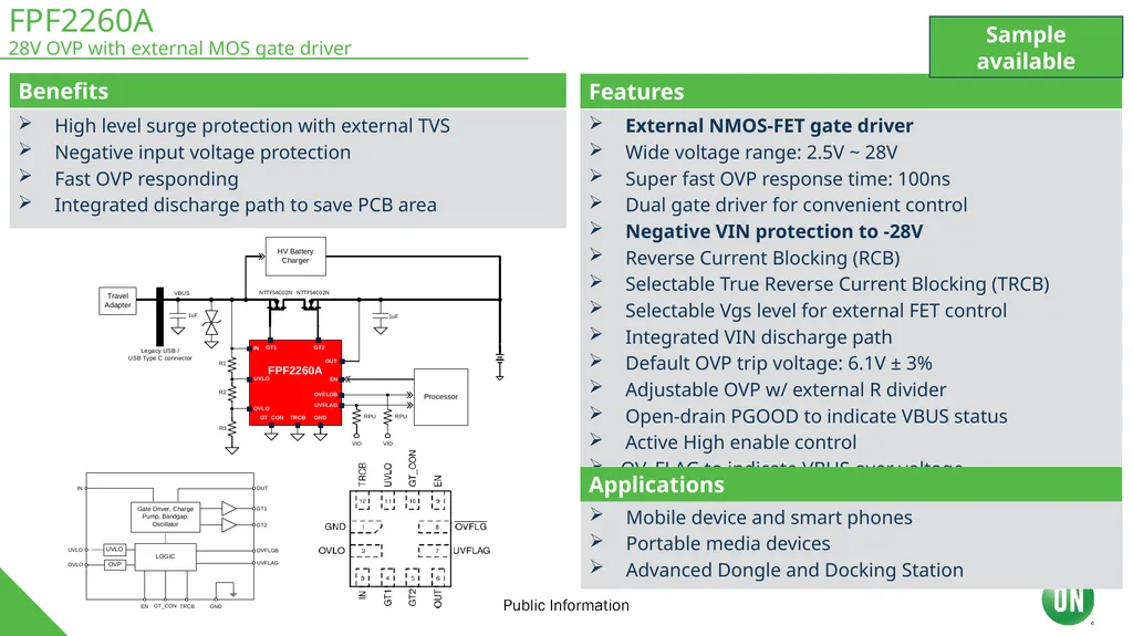
slide2. FPF2260A 28V OVP with external MOS gate driver Features External NMOS-FET gate driver
Wide voltage range: 2.5V ~ 28V
Super fast OVP response time: 100ns
Dual gate driver for convenient control
Negative VIN protection to -28V
Reverse Current Blocking (RCB)
Selectable True Reverse Current Blocking (TRCB)
Selectable Vgs level for external FET control
Integrated VIN discharge path
Default OVP trip voltage: 6.1V ± 3%
Adjustable OVP w/ external R divider
Open-drain PGOOD to indicate VBUS status
Active High enable control
OV_FLAG to indicate VBUS over voltage
Active Low enable control
Package:
TMLP-12, 1.6mm x 1.6mm, 0.4mm pin pitch Mobile device and smart phones
Portable media devices
Advanced Dongle and Docking Station Applications Benefits High level surge protection with external TVS
Negative input voltage protection
Fast OVP responding
Integrated discharge path to save PCB area Sample available<br>
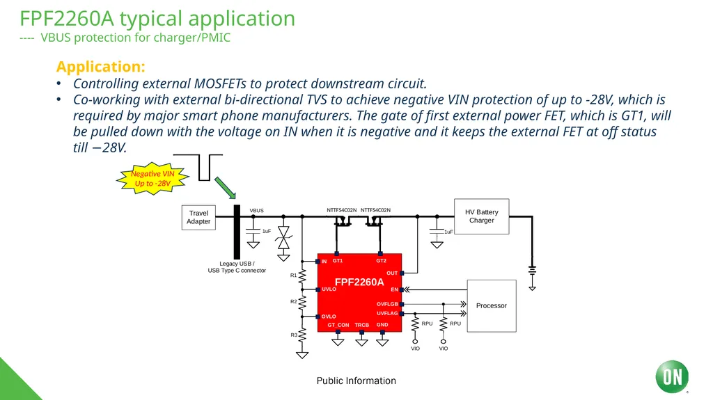
slide3. FPF2260A typical application
---- VBUS protection for charger/PMIC Application:
Controlling external MOSFETs to protect downstream circuit.
Co-working with external bi-directional TVS to achieve negative VIN protection of up to -28V, which is required by major smart phone manufacturers. The gate of first external power FET, which is GT1, will be pulled down with the voltage on IN when it is negative and it keeps the external FET at off status till −28V.<br>
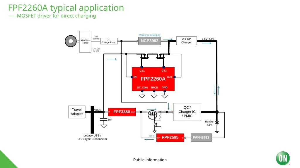
slide4. FPF2260A typical application
---- MOSFET driver for direct charging<br>
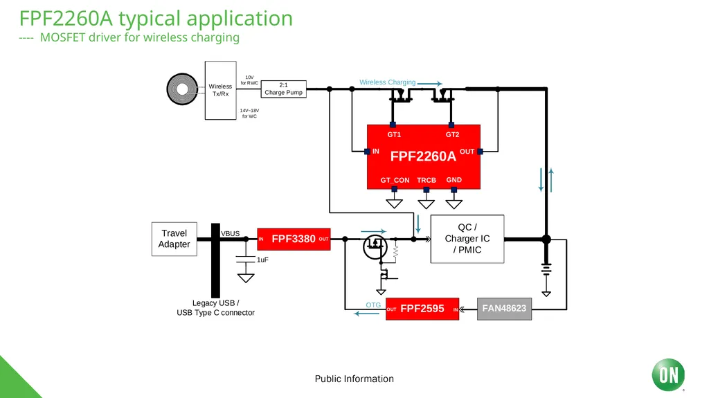
slide5. FPF2260A typical application
---- MOSFET driver for wireless charging<br>
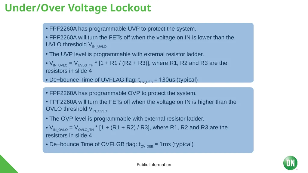
slide6. Under/Over Voltage Lockout FPF2260A has programmable UVP to protect the system.
FPF2260A will turn the FETs off when the voltage on IN is lower than the UVLO threshold VIN_UVLO
The UVP level is programmable with external resistor ladder.
VIN_UVLO = VUVLO_TH * [1 + R1 / (R2 + R3)], where R1, R2 and R3 are the resistors in slide 4
De−bounce Time of UVFLAG flag: tUV_DEB = 130us (typical) FPF2260A has programmable OVP to protect the system.
FPF2260A will turn the FETs off when the voltage on IN is higher than the OVLO threshold VIN_OVLO
The OVP level is programmable with external resistor ladder.
VIN_OVLO = VOVLO_TH * [1 + (R1 + R2) / R3], where R1, R2 and R3 are the resistors in slide 4
De−bounce Time of OVFLGB flag: tOV_DEB = 1ms (typical)<br>
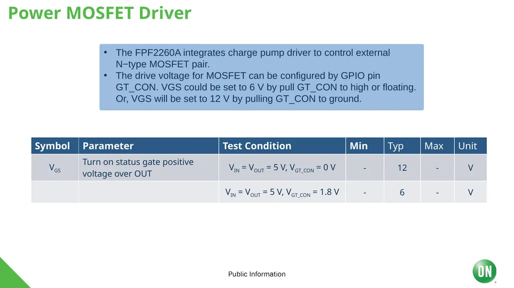
slide7. Power MOSFET Driver The FPF2260A integrates charge pump driver to control external N−type MOSFET pair.
The drive voltage for MOSFET can be configured by GPIO pin GT_CON. VGS could be set to 6 V by pull GT_CON to high or floating. Or, VGS will be set to 12 V by pulling GT_CON to ground.<br>
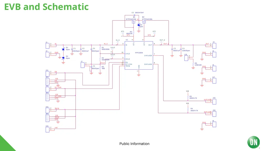
slide8. EVB and Schematic<br>
slide2. FPF2260A 28V OVP with external MOS gate driver Features External NMOS-FET gate driver
Wide voltage range: 2.5V ~ 28V
Super fast OVP response time: 100ns
Dual gate driver for convenient control
Negative VIN protection to -28V
Reverse Current Blocking (RCB)
Selectable True Reverse Current Blocking (TRCB)
Selectable Vgs level for external FET control
Integrated VIN discharge path
Default OVP trip voltage: 6.1V ± 3%
Adjustable OVP w/ external R divider
Open-drain PGOOD to indicate VBUS status
Active High enable control
OV_FLAG to indicate VBUS over voltage
Active Low enable control
Package:
TMLP-12, 1.6mm x 1.6mm, 0.4mm pin pitch Mobile device and smart phones
Portable media devices
Advanced Dongle and Docking Station Applications Benefits High level surge protection with external TVS
Negative input voltage protection
Fast OVP responding
Integrated discharge path to save PCB area Sample available<br>
slide3. FPF2260A typical application
---- VBUS protection for charger/PMIC Application:
Controlling external MOSFETs to protect downstream circuit.
Co-working with external bi-directional TVS to achieve negative VIN protection of up to -28V, which is required by major smart phone manufacturers. The gate of first external power FET, which is GT1, will be pulled down with the voltage on IN when it is negative and it keeps the external FET at off status till −28V.<br>
slide4. FPF2260A typical application
---- MOSFET driver for direct charging<br>
slide5. FPF2260A typical application
---- MOSFET driver for wireless charging<br>
slide6. Under/Over Voltage Lockout FPF2260A has programmable UVP to protect the system.
FPF2260A will turn the FETs off when the voltage on IN is lower than the UVLO threshold VIN_UVLO
The UVP level is programmable with external resistor ladder.
VIN_UVLO = VUVLO_TH * [1 + R1 / (R2 + R3)], where R1, R2 and R3 are the resistors in slide 4
De−bounce Time of UVFLAG flag: tUV_DEB = 130us (typical) FPF2260A has programmable OVP to protect the system.
FPF2260A will turn the FETs off when the voltage on IN is higher than the OVLO threshold VIN_OVLO
The OVP level is programmable with external resistor ladder.
VIN_OVLO = VOVLO_TH * [1 + (R1 + R2) / R3], where R1, R2 and R3 are the resistors in slide 4
De−bounce Time of OVFLGB flag: tOV_DEB = 1ms (typical)<br>
slide7. Power MOSFET Driver The FPF2260A integrates charge pump driver to control external N−type MOSFET pair.
The drive voltage for MOSFET can be configured by GPIO pin GT_CON. VGS could be set to 6 V by pull GT_CON to high or floating. Or, VGS will be set to 12 V by pulling GT_CON to ground.<br>
slide8. EVB and Schematic<br>