Gates and Logic: From switches to Transistors,
Description: Gates and Logic: From switches to Transistors, Logic Gates and Logic Circuits Hakim Weatherspoon CS 3410, Spring 2013 Computer Science Cornell University See: PH Appendix C.2 and C.3 (Also, see C.0 and C.1) Goals for Today From Switches to
Related Topics
Download Presentation
"Gates and Logic: From switches to Transistors," is the property of its rightful owner. Permission is granted to download and print the materials on this website for personal, non-commercial use only, and to display it on your personal computer provided you do not modify the materials and that you retain all copyright notices contained in the materials. By downloading content from our website, you accept the terms of this agreement.
Presentation Transcript
slide1. Gates and Logic:From switches to Transistors, Logic Gates and Logic Circuits Hakim Weatherspoon
CS 3410, Spring 2013
Computer Science
Cornell University See: P&H Appendix C.2 and C.3 (Also, see C.0 and C.1)<br>
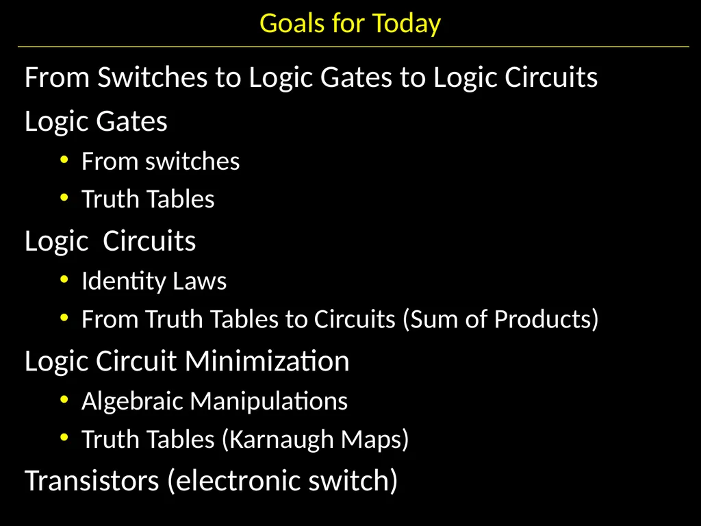
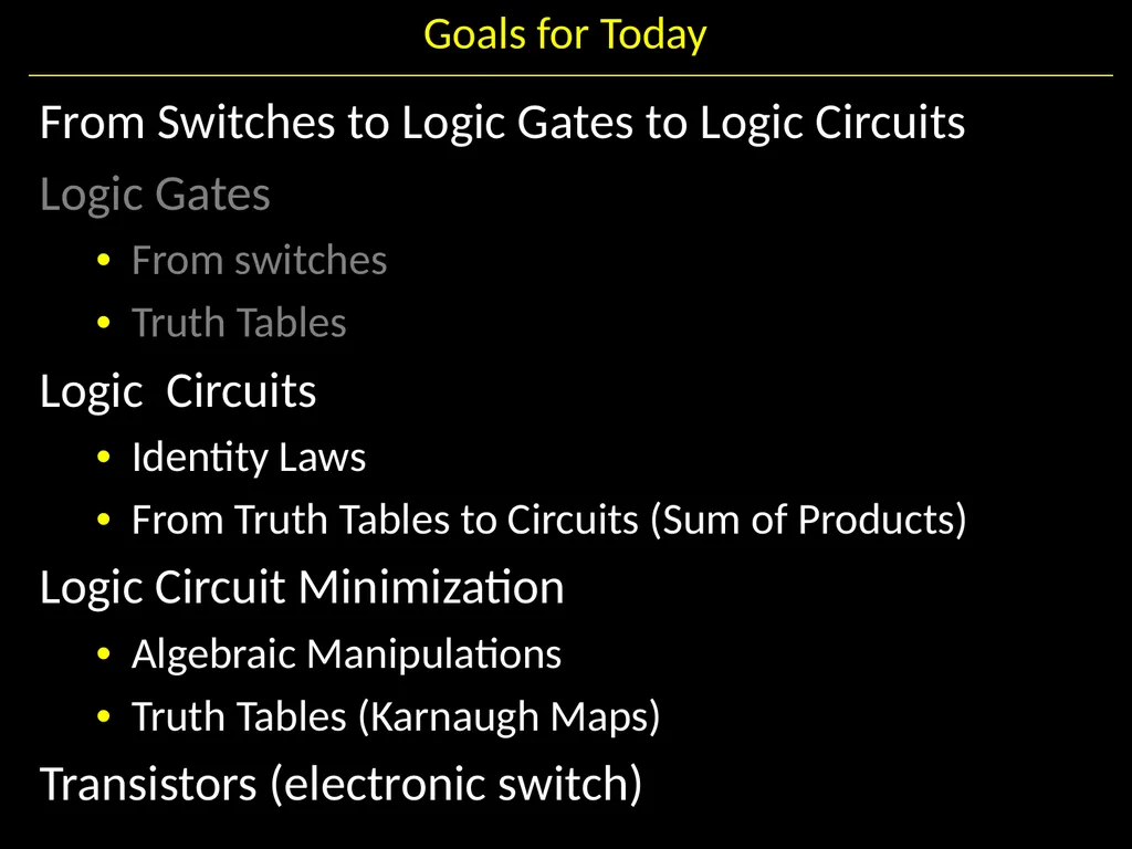
slide2. Goals for Today From Switches to Logic Gates to Logic Circuits
Logic Gates
From switches
Truth Tables
Logic Circuits
Identity Laws
From Truth Tables to Circuits (Sum of Products)
Logic Circuit Minimization
Algebraic Manipulations
Truth Tables (Karnaugh Maps)
Transistors (electronic switch)<br>
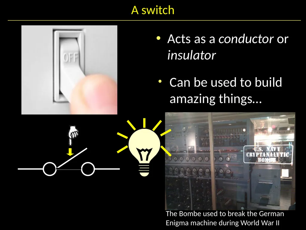
slide3. A switch Acts as a conductor or insulator Can be used to build amazing things… The Bombe used to break the German
Enigma machine during World War II<br>
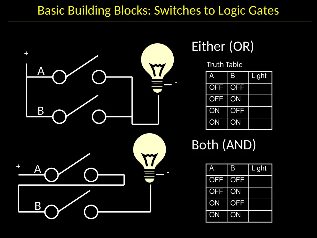
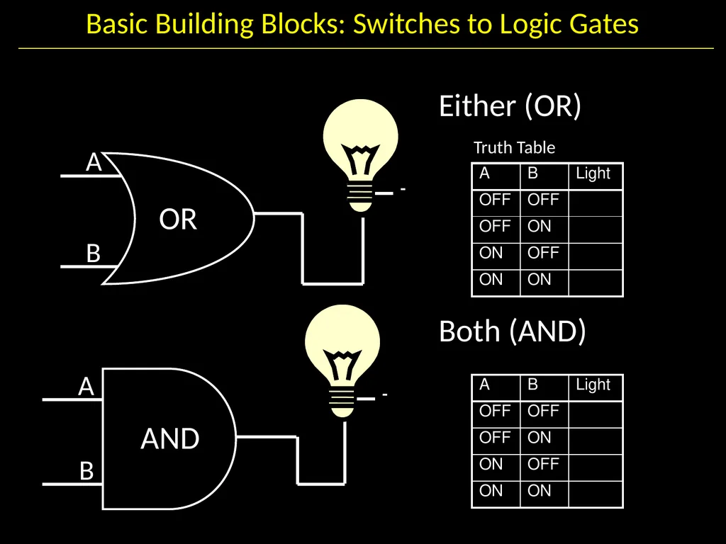
slide4. Basic Building Blocks: Switches to Logic Gates Either (OR)
Both (AND) + - - A B A B Truth Table +<br>
slide5. Basic Building Blocks: Switches to Logic Gates Either (OR)
Both (AND) - - A B A B Truth Table OR AND<br>
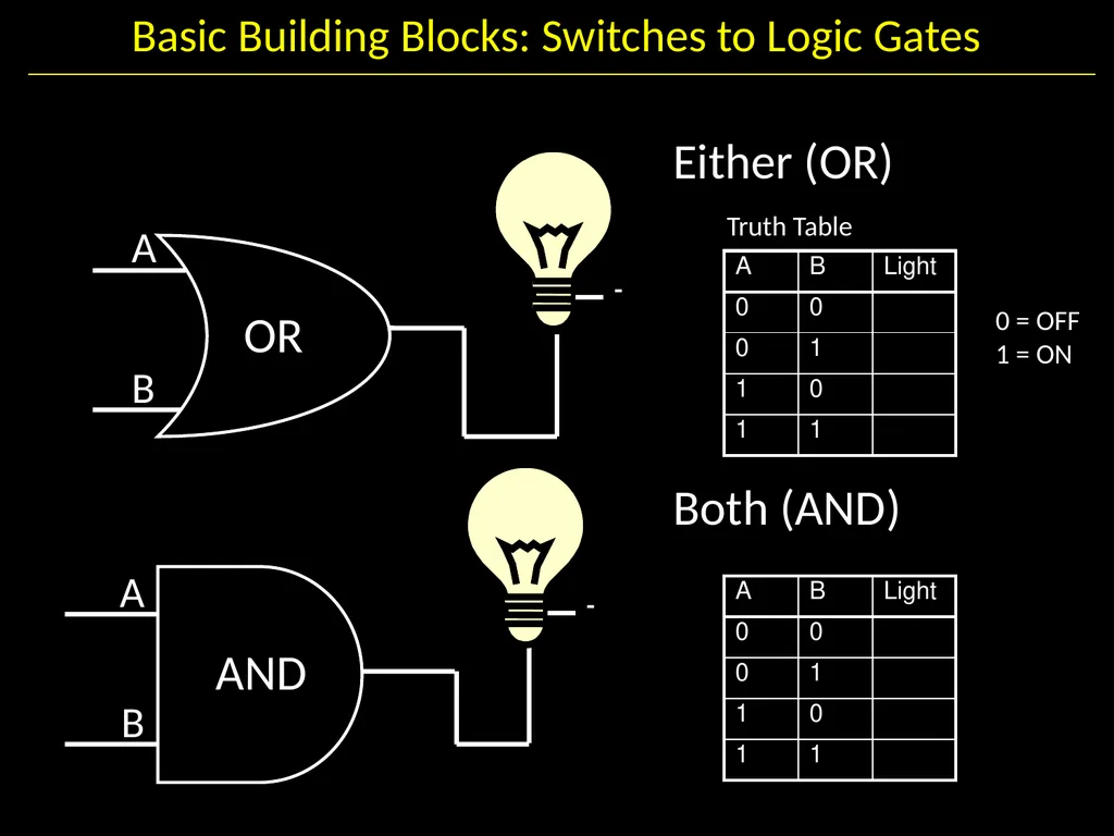
slide6. Basic Building Blocks: Switches to Logic Gates Either (OR)
Both (AND) - - A B A B Truth Table 0 = OFF
1 = ON OR AND<br>
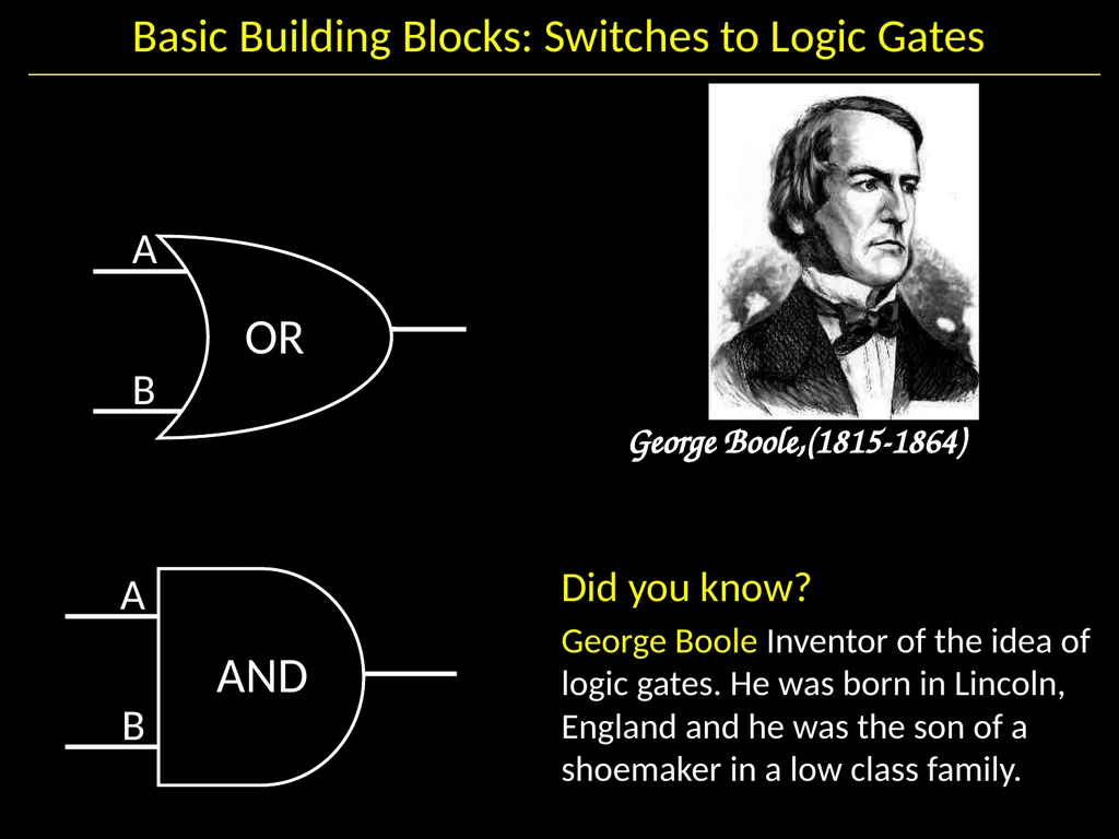
slide7. Basic Building Blocks: Switches to Logic Gates Did you know?
George Boole Inventor of the idea of logic gates. He was born in Lincoln, England and he was the son of a shoemaker in a low class family. A B A B George Boole,(1815-1864) OR AND<br>
slide8. Takeaway Binary (two symbols: true and false) is the basis of Logic Design<br>
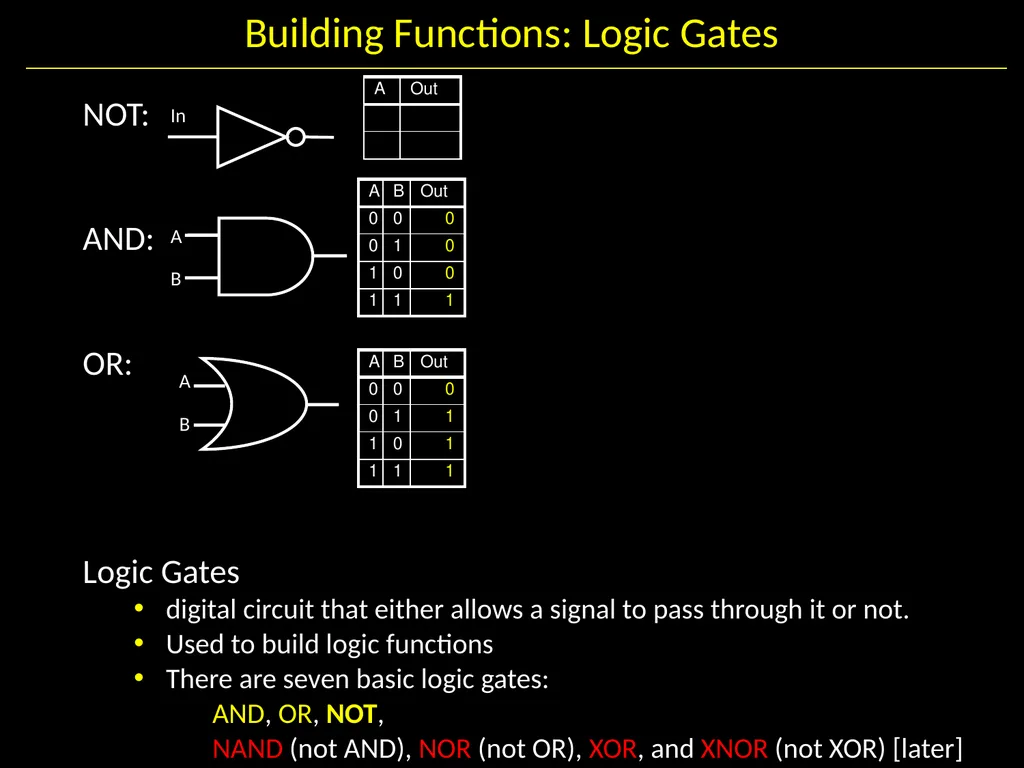
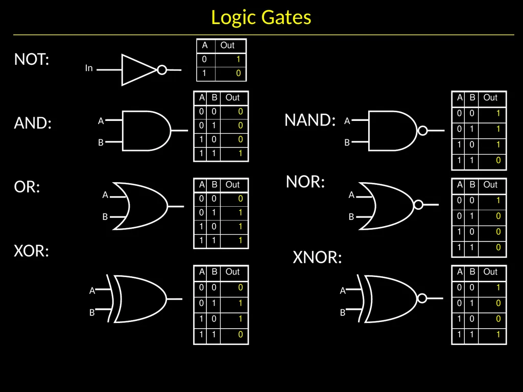
slide9. Building Functions: Logic Gates NOT:
AND:
OR:
Logic Gates
digital circuit that either allows a signal to pass through it or not.
Used to build logic functions
There are seven basic logic gates:
AND, OR, NOT,
NAND (not AND), NOR (not OR), XOR, and XNOR (not XOR) [later] A B A B In<br>
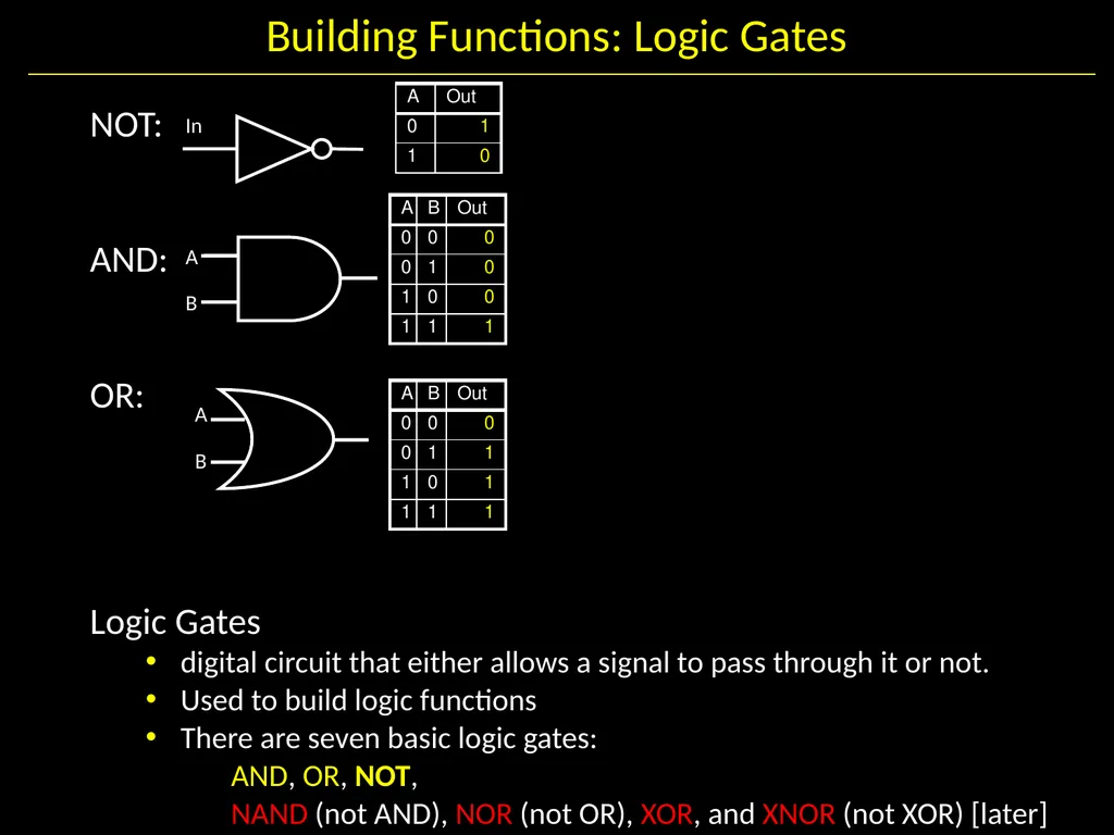
slide10. Building Functions: Logic Gates NOT:
AND:
OR:
Logic Gates
digital circuit that either allows a signal to pass through it or not.
Used to build logic functions
There are seven basic logic gates:
AND, OR, NOT,
NAND (not AND), NOR (not OR), XOR, and XNOR (not XOR) [later] A B A B In<br>
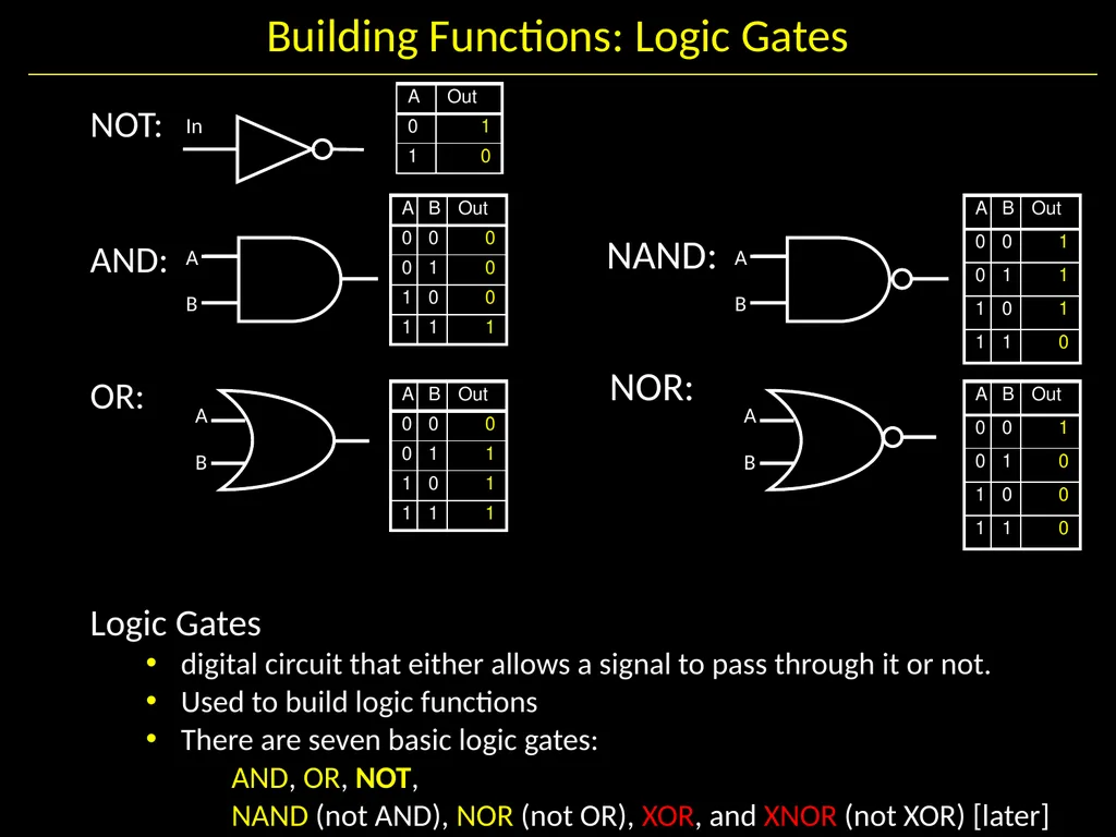
slide11. NOT:
AND:
OR:
Logic Gates
digital circuit that either allows a signal to pass through it or not.
Used to build logic functions
There are seven basic logic gates:
AND, OR, NOT,
NAND (not AND), NOR (not OR), XOR, and XNOR (not XOR) [later] Building Functions: Logic Gates A B A B In NAND: NOR:<br>
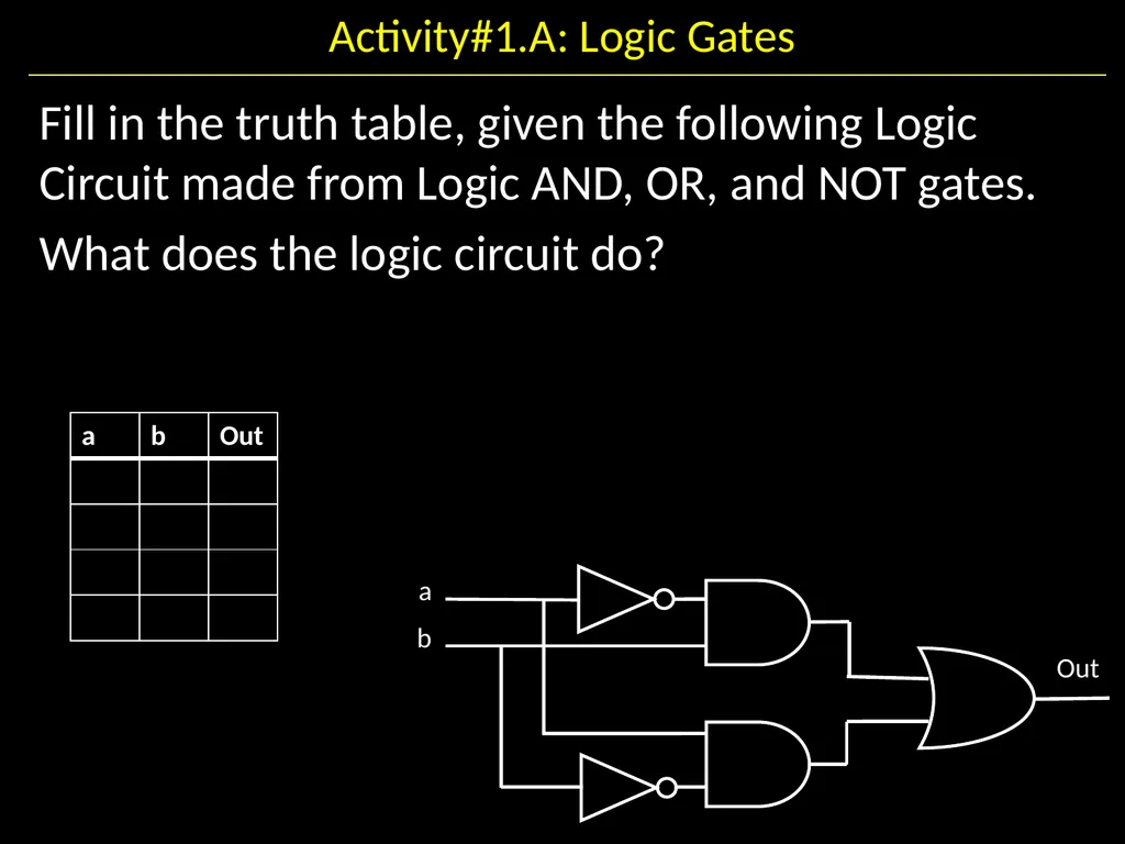
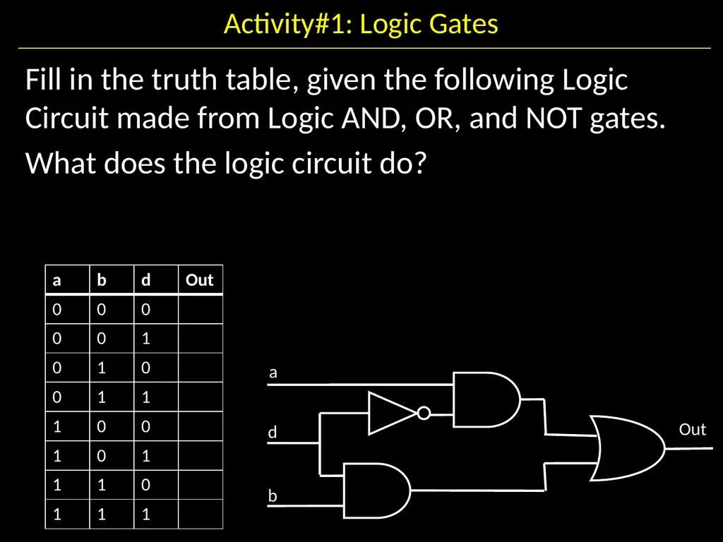
slide12. Fill in the truth table, given the following Logic Circuit made from Logic AND, OR, and NOT gates.
What does the logic circuit do? Activity#1.A: Logic Gates a b Out<br>
slide13. Activity#1: Logic Gates Fill in the truth table, given the following Logic Circuit made from Logic AND, OR, and NOT gates.
What does the logic circuit do?<br>
slide14. Goals for Today From Switches to Logic Gates to Logic Circuits
Logic Gates
From switches
Truth Tables
Logic Circuits
Identity Laws
From Truth Tables to Circuits (Sum of Products)
Logic Circuit Minimization
Algebraic Manipulations
Truth Tables (Karnaugh Maps)
Transistors (electronic switch)<br>
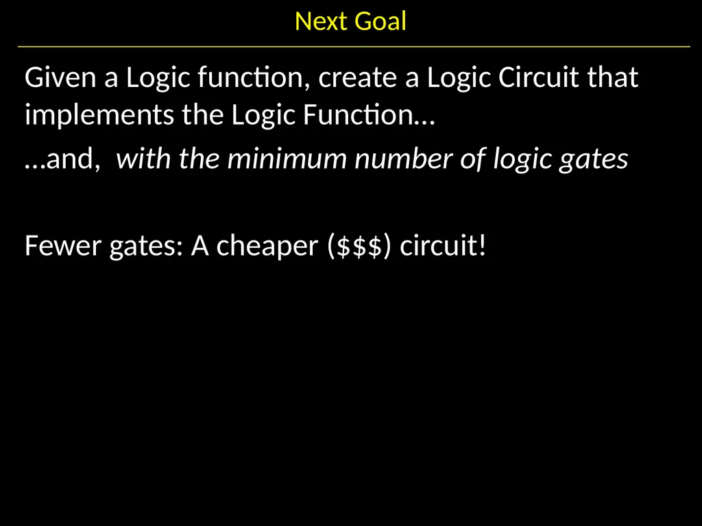
slide15. Next Goal Given a Logic function, create a Logic Circuit that implements the Logic Function…
…and, with the minimum number of logic gates
Fewer gates: A cheaper ($$$) circuit!<br>
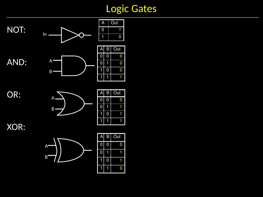
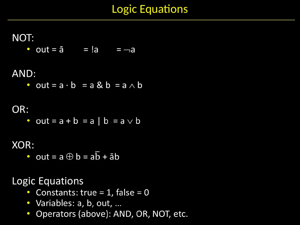
slide16. NOT:
AND:
OR:
XOR:
L
ogic Equations
Constants: true = 1, false = 0
Variables: a, b, out, …
Operators (above): AND, OR, NOT, etc. Logic Gates A B A B In A B<br>
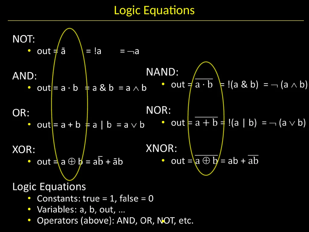
slide17. NOT:
AND:
OR:
XOR:
L
ogic Equations
Constants: true = 1, false = 0
Variables: a, b, out, …
Operators (above): AND, OR, NOT, etc. Logic Gates A B A B In A B NAND: NOR: XNOR:<br>
slide18. Logic Equations<br>
slide19. Logic Equations<br>
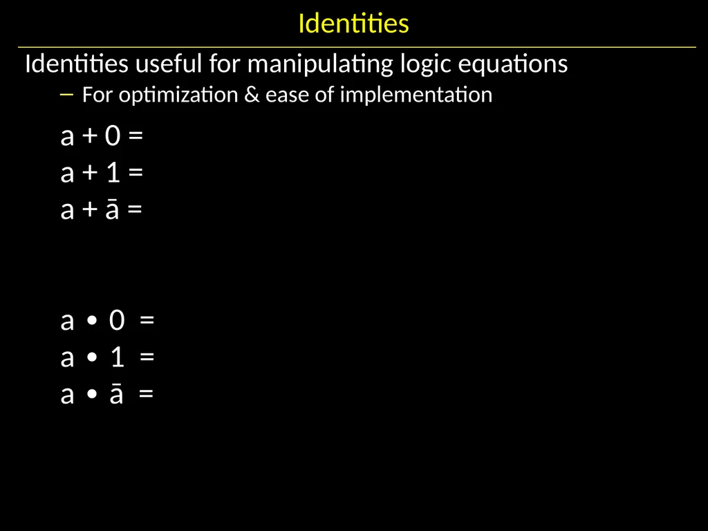
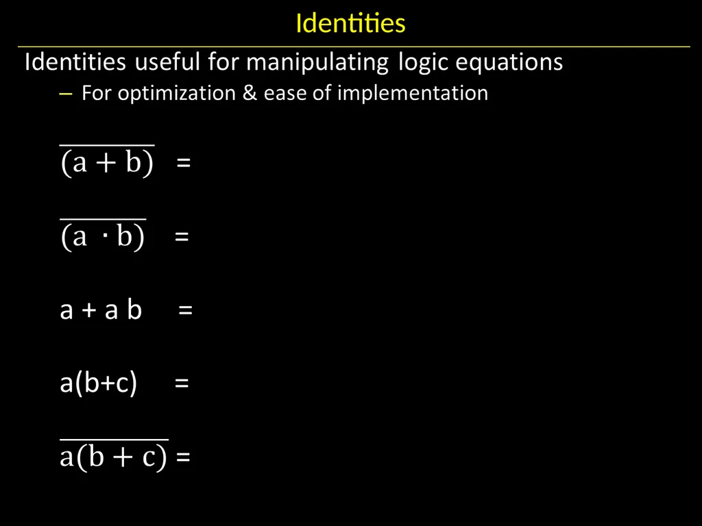
slide20. Identities Identities useful for manipulating logic equations
For optimization & ease of implementation
a + 0 =
a + 1 =
a + ā =
a ∙ 0 =
a ∙ 1 =
a ∙ ā =<br>
slide21. Identities<br>
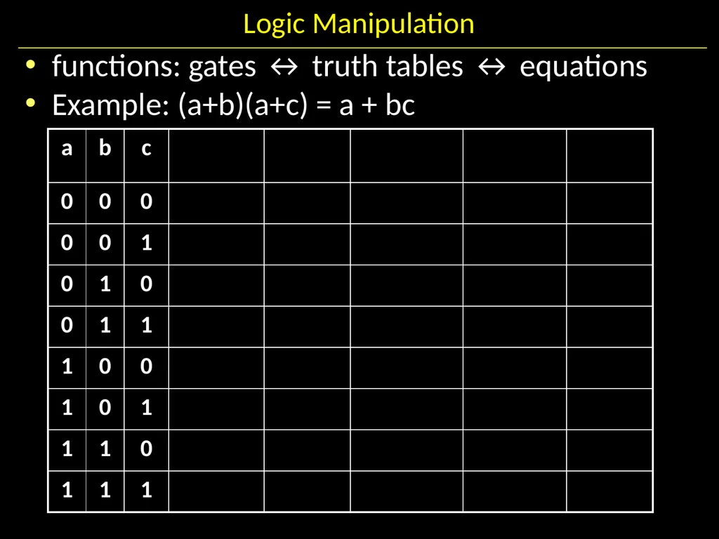
slide22. Logic Manipulation functions: gates ↔ truth tables ↔ equations
Example: (a+b)(a+c) = a + bc<br>
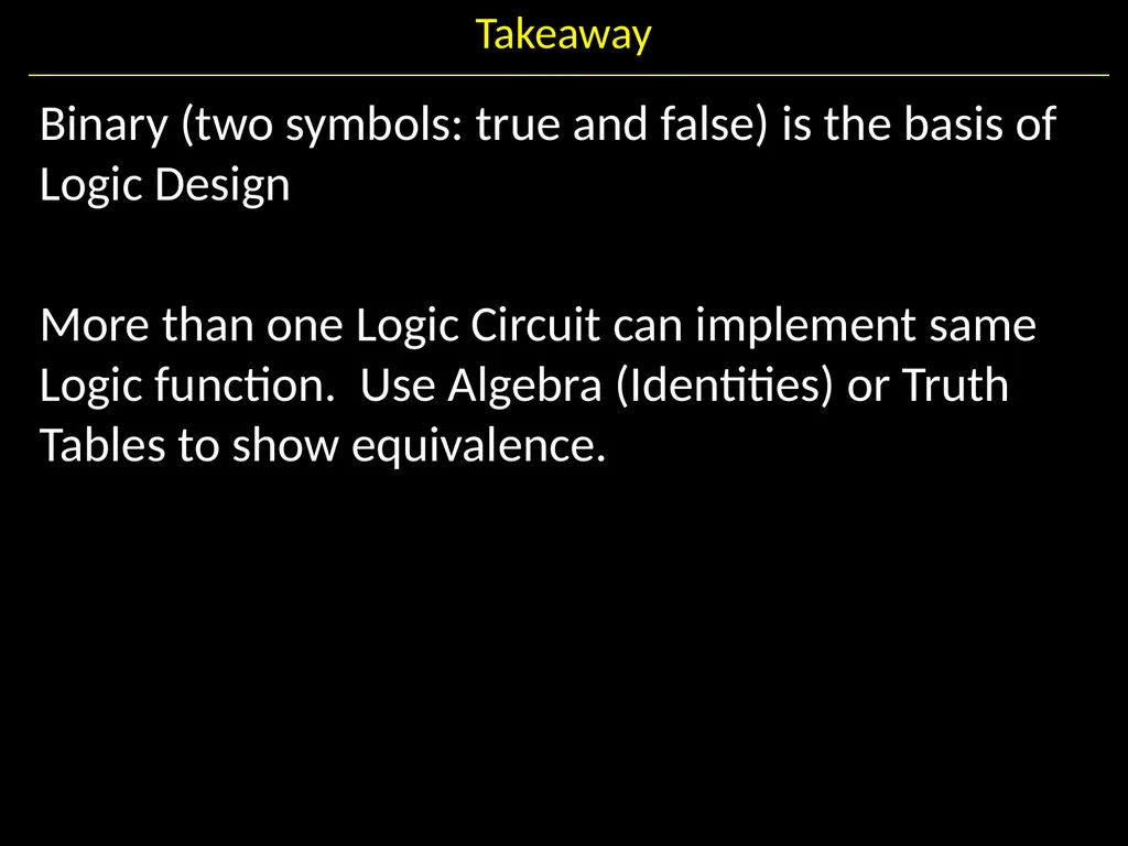
slide23. Takeaway Binary (two symbols: true and false) is the basis of Logic Design
More than one Logic Circuit can implement same Logic function. Use Algebra (Identities) or Truth Tables to show equivalence.<br>
slide25. Next Goal How to standardize minimizing logic circuits?<br>
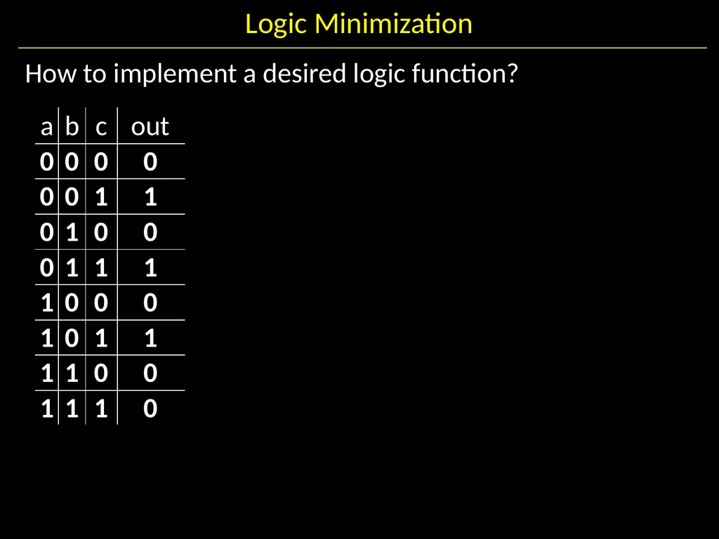
slide26. Logic Minimization How to implement a desired logic function?<br>
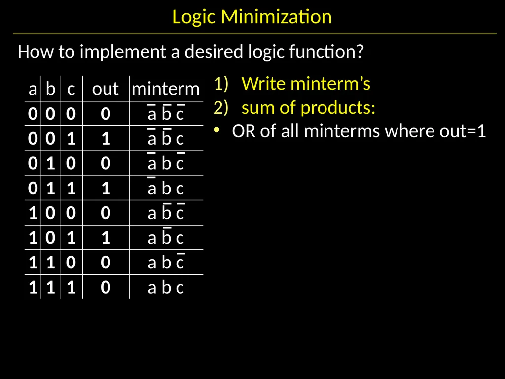
slide27. Logic Minimization How to implement a desired logic function? Write minterm’s
sum of products:
OR of all minterms where out=1<br>
slide28. Karnaugh Maps How does one find the most efficient equation?
Manipulate algebraically until…?
Use Karnaugh maps (optimize visually)
Use a software optimizer
For large circuits
Decomposition & reuse of building blocks<br>
slide29. Sum of minterms yields?
out = Minimization with Karnaugh maps (1)<br>
slide30. Sum of minterms yields?
out =
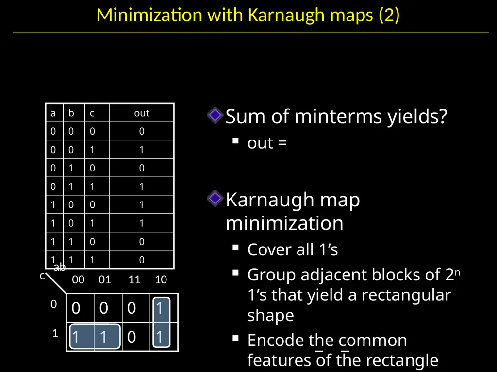
Karnaugh maps identify which inputs are (ir)relevant to the output 00 01 11 10 0 1 c ab Minimization with Karnaugh maps (2)<br>
slide31. Sum of minterms yields?
out =
Karnaugh map minimization
Cover all 1’s
Group adjacent blocks of 2n 1’s that yield a rectangular shape
Encode the common features of the rectangle
out = ab + ac 00 01 11 10 0 1 c ab Minimization with Karnaugh maps (2)<br>
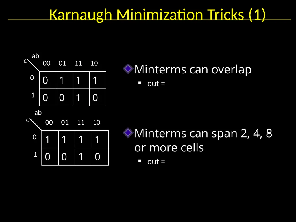
slide32. Karnaugh Minimization Tricks (1) Minterms can overlap
out =
Minterms can span 2, 4, 8 or more cells
out = 00 01 11 10 0 1 c ab 00 01 11 10 0 1 c ab<br>
slide33. Karnaugh Minimization Tricks (2) The map wraps around
out =
out = 00 01 11 10 00 01 ab cd 11 10 00 01 11 10 00 01 ab cd 11 10<br>
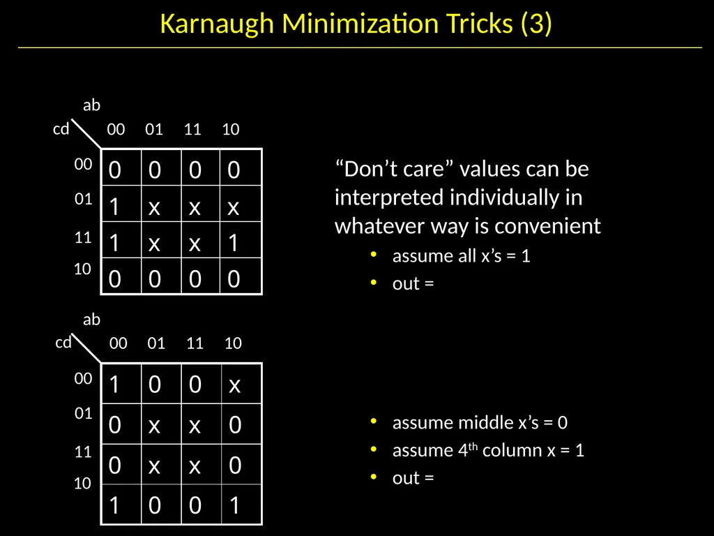
slide34. Karnaugh Minimization Tricks (3) “Don’t care” values can be interpreted individually in whatever way is convenient
assume all x’s = 1
out =
assume middle x’s = 0
assume 4th column x = 1
out = 00 01 11 10 00 01 ab cd 11 10 00 01 11 10 00 01 ab cd 11 10<br>
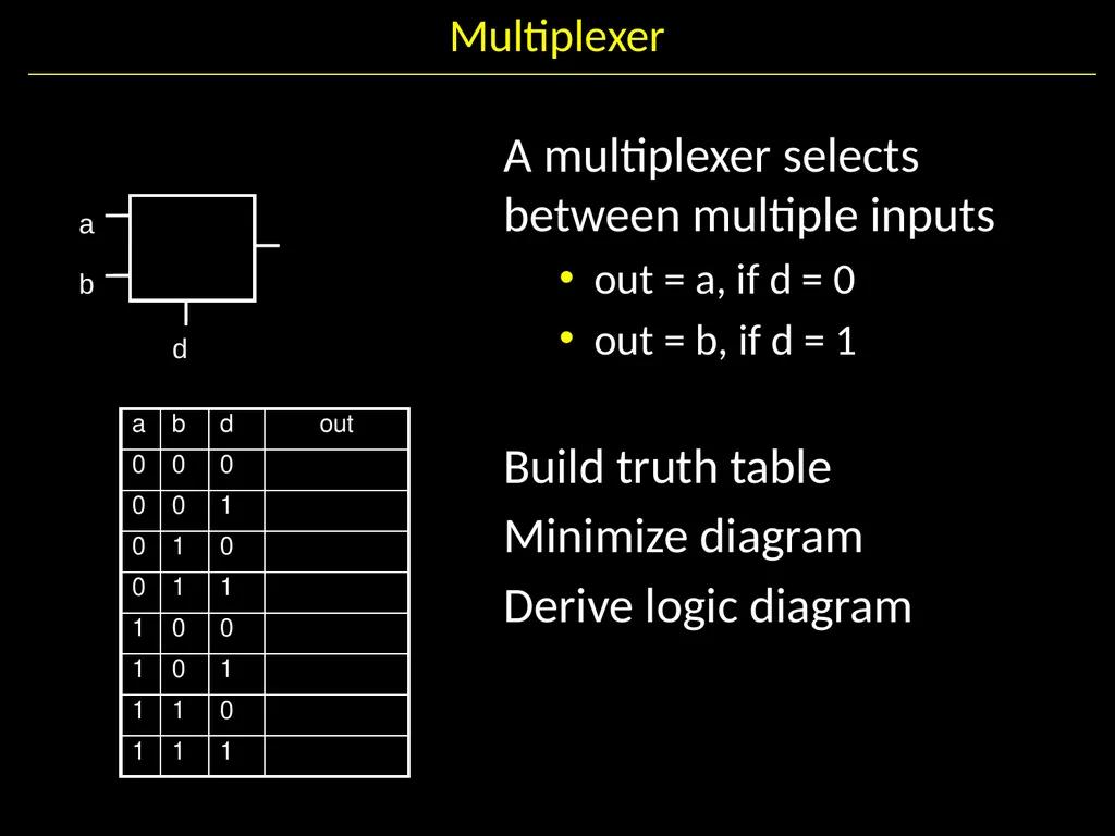
slide35. Multiplexer A multiplexer selects between multiple inputs
out = a, if d = 0
out = b, if d = 1
Build truth table
Minimize diagram
Derive logic diagram<br>
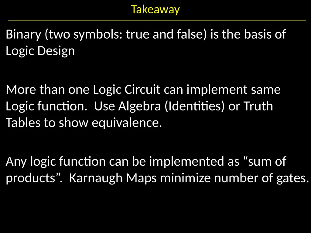
slide36. Takeaway Binary (two symbols: true and false) is the basis of Logic Design
More than one Logic Circuit can implement same Logic function. Use Algebra (Identities) or Truth Tables to show equivalence.
Any logic function can be implemented as “sum of products”. Karnaugh Maps minimize number of gates.<br>
slide37. Goals for Today From Transistors to Gates to Logic Circuits
Logic Gates
From transistors
Truth Tables
Logic Circuits
Identity Laws
From Truth Tables to Circuits (Sum of Products)
Logic Circuit Minimization
Algebraic Manipulations
Truth Tables (Karnaugh Maps)
Transistors (electronic switch)<br>
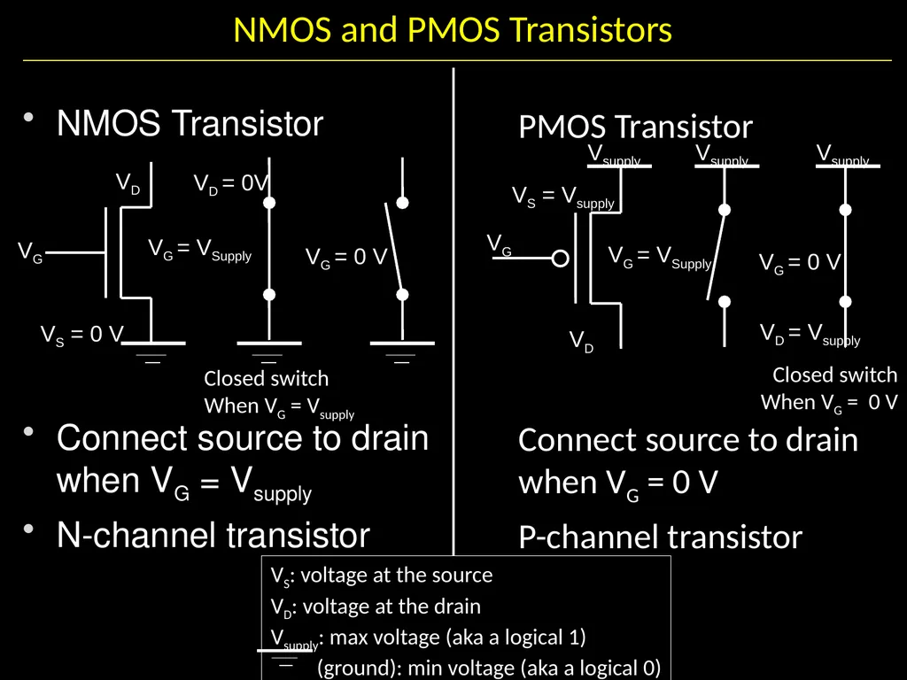
slide38. NMOS Transistor
Connect source to drain when VG = Vsupply
N-channel transistor VS = 0 V VG VG = VSupply VG = 0 V NMOS and PMOS Transistors PMOS Transistor
Connect source to drain when VG = 0 V
P-channel transistor VG VG = VSupply VG = 0 V VD VD = 0V Closed switch
When VG = Vsupply Closed switch
When VG = 0 V Vsupply VS = Vsupply Vsupply Vsupply VD VD = Vsupply<br>
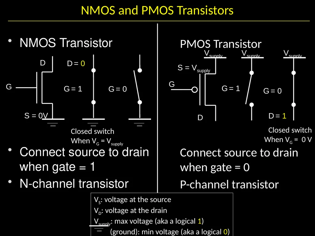
slide39. NMOS Transistor
Connect source to drain when gate = 1
N-channel transistor D S = 0V G G = 1 G = 0 NMOS and PMOS Transistors PMOS Transistor
Connect source to drain when gate = 0
P-channel transistor Vsupply D G G = 1 G = 0 D = 0 Closed switch
When VG = Vsupply Closed switch
When VG = 0 V S = Vsupply Vsupply Vsupply D = 1<br>
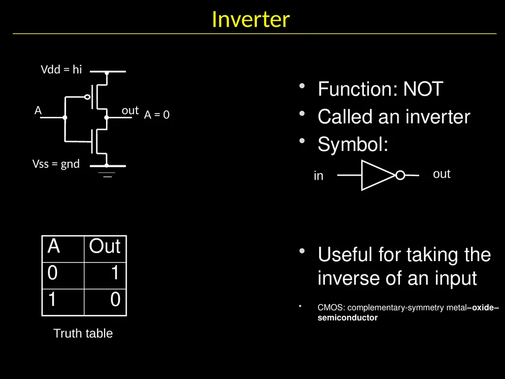
slide40. Inverter Function: NOT
Called an inverter
Symbol:
Useful for taking the inverse of an input
CMOS: complementary-symmetry metal–oxide–semiconductor in out Truth table A out Vdd = hi Vss = gnd A = 0<br>
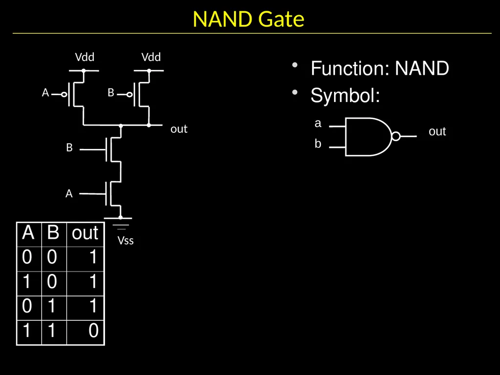
slide41. NAND Gate Function: NAND
Symbol: b a out A out Vdd B B A Vdd Vss<br>
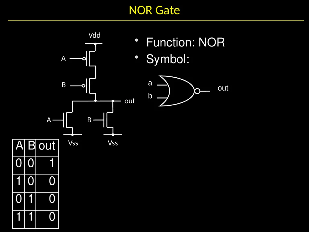
slide42. NOR Gate A out Vss Vdd B B A Vss b a out Function: NOR
Symbol:<br>
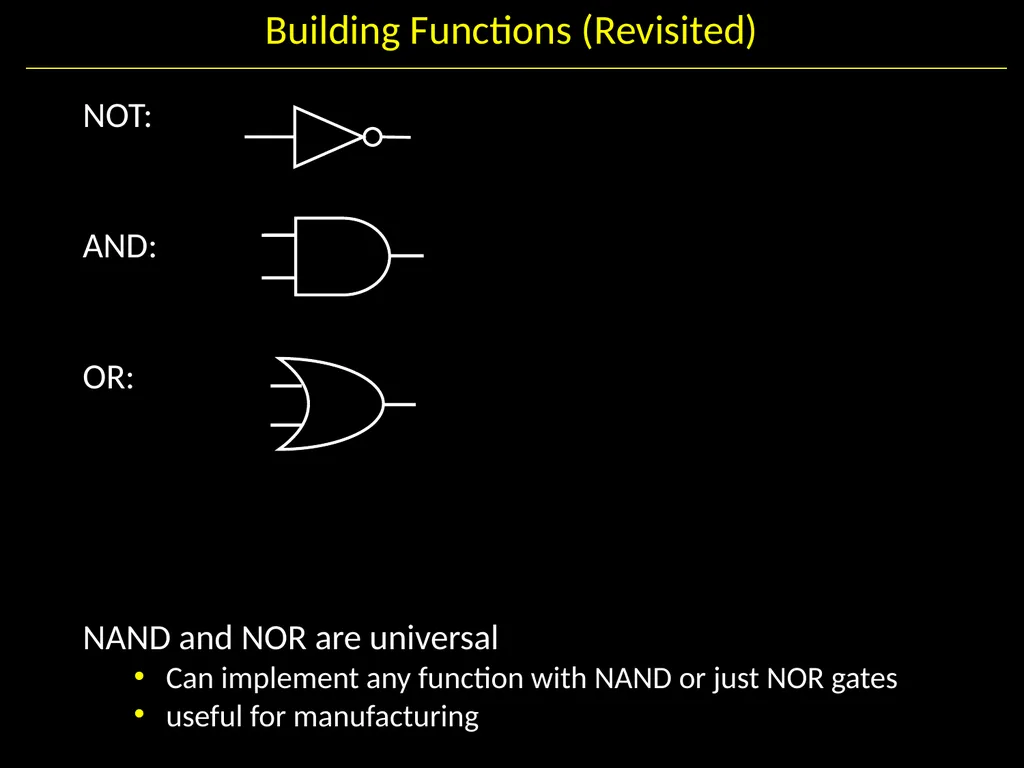
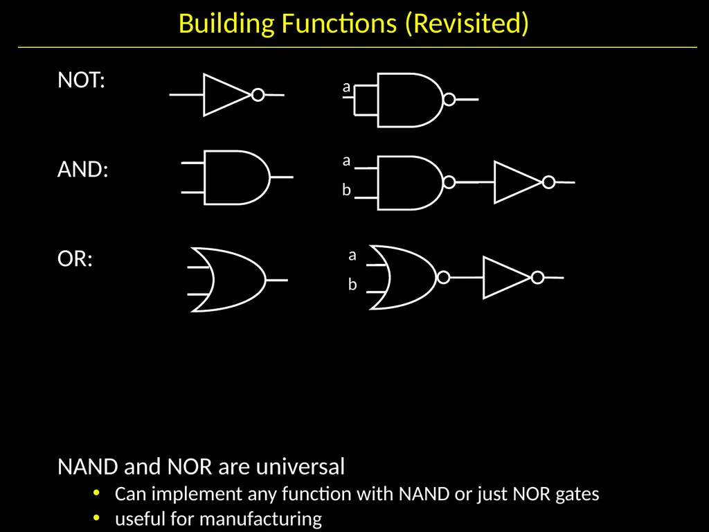
slide43. Building Functions (Revisited) NOT:
AND:
OR:
NAND and NOR are universal
Can implement any function with NAND or just NOR gates
useful for manufacturing<br>
slide44. Building Functions (Revisited) NOT:
AND:
OR:
NAND and NOR are universal
Can implement any function with NAND or just NOR gates
useful for manufacturing b a b a a<br>
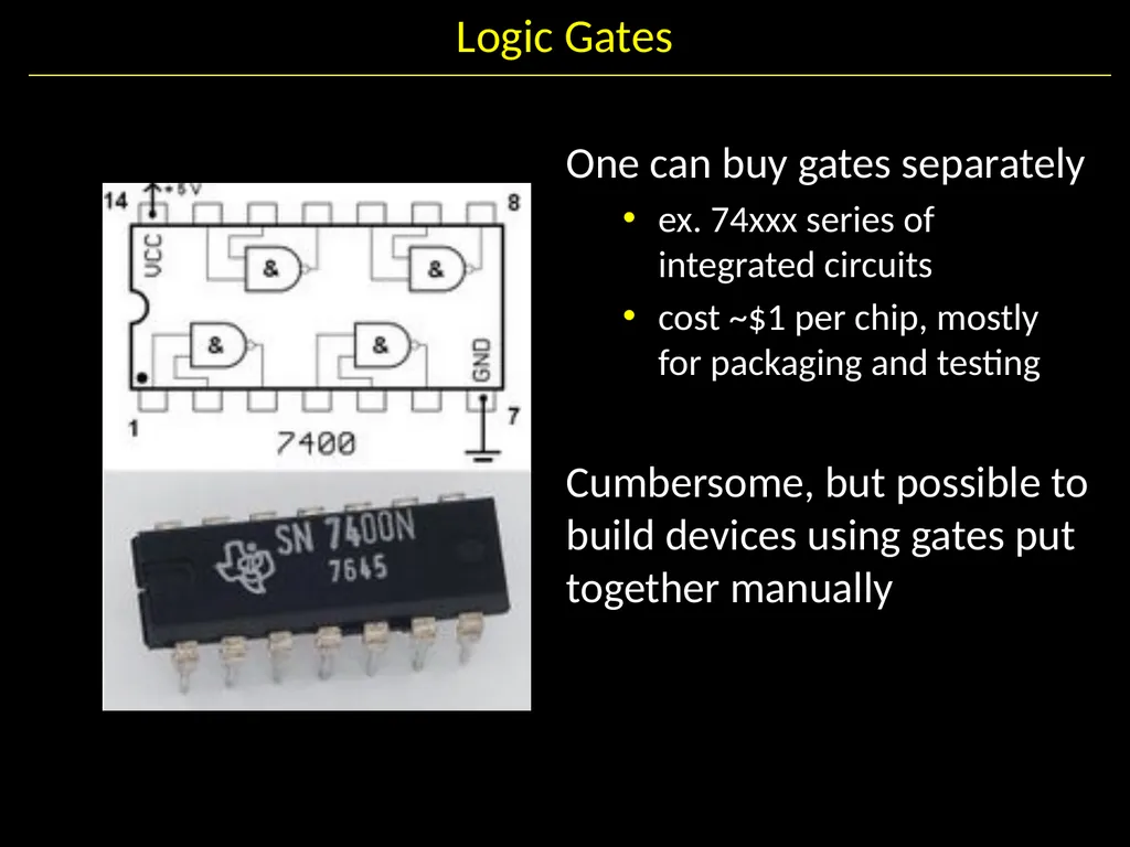
slide45. Logic Gates One can buy gates separately
ex. 74xxx series of integrated circuits
cost ~$1 per chip, mostly for packaging and testing
Cumbersome, but possible to build devices using gates put together manually<br>
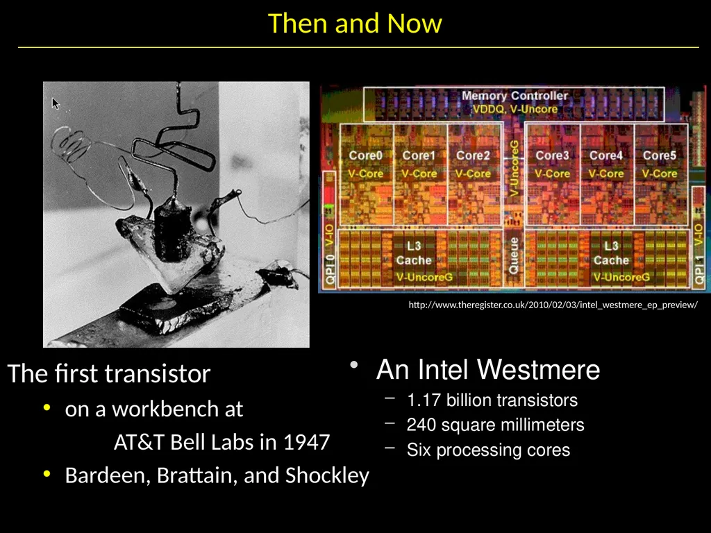
slide46. Then and Now The first transistor
on a workbench at
AT&T Bell Labs in 1947
Bardeen, Brattain, and Shockley An Intel Westmere
1.17 billion transistors
240 square millimeters
Six processing cores http://www.theregister.co.uk/2010/02/03/intel_westmere_ep_preview/<br>
slide47. Summary Most modern devices are made from billions of on /off switches called transistors
We will build a processor in this course!
Transistors made from semiconductor materials:
MOSFET – Metal Oxide Semiconductor Field Effect Transistor
NMOS, PMOS – Negative MOS and Positive MOS
CMOS – Complimentary MOS made from PMOS and NMOS transistors
Transistors used to make logic gates and logic circuits
We can now implement any logic circuit
Can do it efficiently, using Karnaugh maps to find the minimal terms required
Can use either NAND or NOR gates to implement the logic circuit
Can use P- and N-transistors to implement NAND or NOR gates<br>
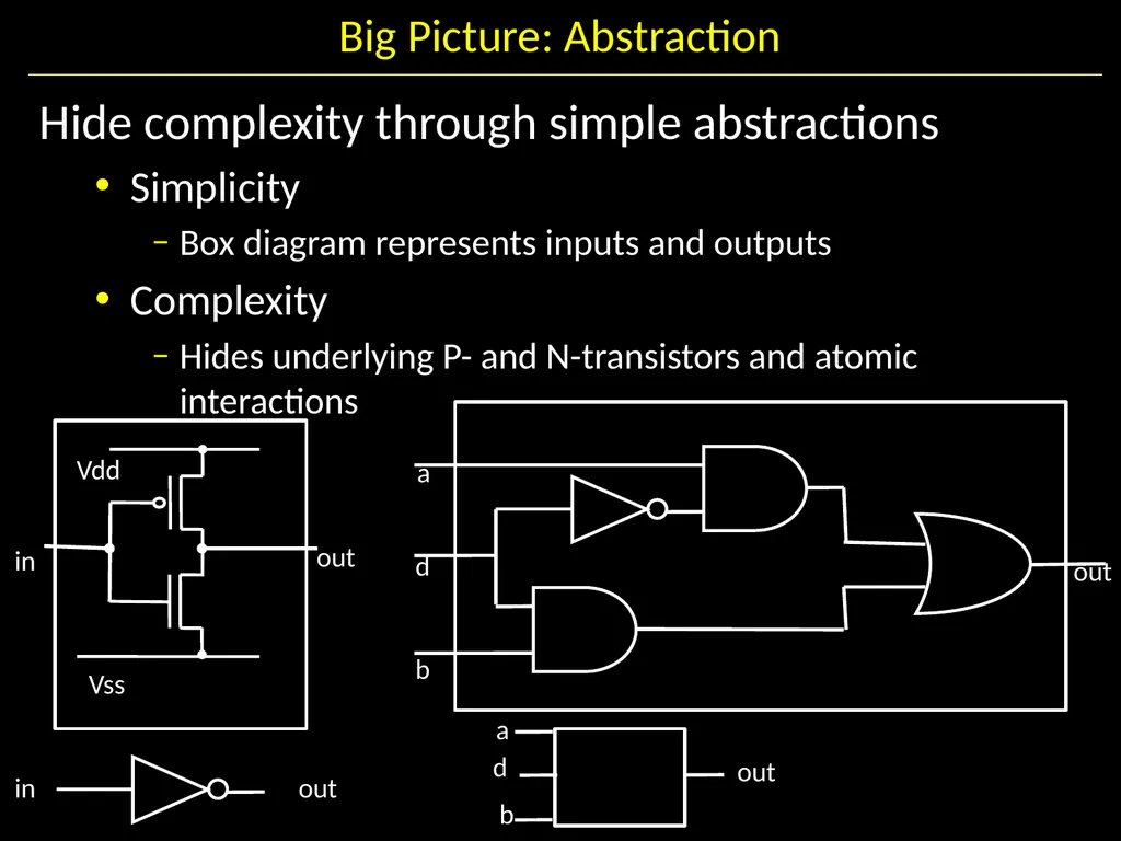
slide48. Big Picture: Abstraction Hide complexity through simple abstractions
Simplicity
Box diagram represents inputs and outputs
Complexity
Hides underlying P- and N-transistors and atomic interactions<br>

CS 3410, Spring 2013
Computer Science
Cornell University See: P&H Appendix C.2 and C.3 (Also, see C.0 and C.1)<br>
slide2. Goals for Today From Switches to Logic Gates to Logic Circuits
Logic Gates
From switches
Truth Tables
Logic Circuits
Identity Laws
From Truth Tables to Circuits (Sum of Products)
Logic Circuit Minimization
Algebraic Manipulations
Truth Tables (Karnaugh Maps)
Transistors (electronic switch)<br>
slide3. A switch Acts as a conductor or insulator Can be used to build amazing things… The Bombe used to break the German
Enigma machine during World War II<br>
slide4. Basic Building Blocks: Switches to Logic Gates Either (OR)
Both (AND) + - - A B A B Truth Table +<br>
slide5. Basic Building Blocks: Switches to Logic Gates Either (OR)
Both (AND) - - A B A B Truth Table OR AND<br>
slide6. Basic Building Blocks: Switches to Logic Gates Either (OR)
Both (AND) - - A B A B Truth Table 0 = OFF
1 = ON OR AND<br>
slide7. Basic Building Blocks: Switches to Logic Gates Did you know?
George Boole Inventor of the idea of logic gates. He was born in Lincoln, England and he was the son of a shoemaker in a low class family. A B A B George Boole,(1815-1864) OR AND<br>
slide8. Takeaway Binary (two symbols: true and false) is the basis of Logic Design<br>
slide9. Building Functions: Logic Gates NOT:
AND:
OR:
Logic Gates
digital circuit that either allows a signal to pass through it or not.
Used to build logic functions
There are seven basic logic gates:
AND, OR, NOT,
NAND (not AND), NOR (not OR), XOR, and XNOR (not XOR) [later] A B A B In<br>
slide10. Building Functions: Logic Gates NOT:
AND:
OR:
Logic Gates
digital circuit that either allows a signal to pass through it or not.
Used to build logic functions
There are seven basic logic gates:
AND, OR, NOT,
NAND (not AND), NOR (not OR), XOR, and XNOR (not XOR) [later] A B A B In<br>
slide11. NOT:
AND:
OR:
Logic Gates
digital circuit that either allows a signal to pass through it or not.
Used to build logic functions
There are seven basic logic gates:
AND, OR, NOT,
NAND (not AND), NOR (not OR), XOR, and XNOR (not XOR) [later] Building Functions: Logic Gates A B A B In NAND: NOR:<br>
slide12. Fill in the truth table, given the following Logic Circuit made from Logic AND, OR, and NOT gates.
What does the logic circuit do? Activity#1.A: Logic Gates a b Out<br>
slide13. Activity#1: Logic Gates Fill in the truth table, given the following Logic Circuit made from Logic AND, OR, and NOT gates.
What does the logic circuit do?<br>
slide14. Goals for Today From Switches to Logic Gates to Logic Circuits
Logic Gates
From switches
Truth Tables
Logic Circuits
Identity Laws
From Truth Tables to Circuits (Sum of Products)
Logic Circuit Minimization
Algebraic Manipulations
Truth Tables (Karnaugh Maps)
Transistors (electronic switch)<br>
slide15. Next Goal Given a Logic function, create a Logic Circuit that implements the Logic Function…
…and, with the minimum number of logic gates
Fewer gates: A cheaper ($$$) circuit!<br>
slide16. NOT:
AND:
OR:
XOR:
L
ogic Equations
Constants: true = 1, false = 0
Variables: a, b, out, …
Operators (above): AND, OR, NOT, etc. Logic Gates A B A B In A B<br>
slide17. NOT:
AND:
OR:
XOR:
L
ogic Equations
Constants: true = 1, false = 0
Variables: a, b, out, …
Operators (above): AND, OR, NOT, etc. Logic Gates A B A B In A B NAND: NOR: XNOR:<br>
slide18. Logic Equations<br>
slide19. Logic Equations<br>
slide20. Identities Identities useful for manipulating logic equations
For optimization & ease of implementation
a + 0 =
a + 1 =
a + ā =
a ∙ 0 =
a ∙ 1 =
a ∙ ā =<br>
slide21. Identities<br>
slide22. Logic Manipulation functions: gates ↔ truth tables ↔ equations
Example: (a+b)(a+c) = a + bc<br>
slide23. Takeaway Binary (two symbols: true and false) is the basis of Logic Design
More than one Logic Circuit can implement same Logic function. Use Algebra (Identities) or Truth Tables to show equivalence.<br>
slide25. Next Goal How to standardize minimizing logic circuits?<br>
slide26. Logic Minimization How to implement a desired logic function?<br>
slide27. Logic Minimization How to implement a desired logic function? Write minterm’s
sum of products:
OR of all minterms where out=1<br>
slide28. Karnaugh Maps How does one find the most efficient equation?
Manipulate algebraically until…?
Use Karnaugh maps (optimize visually)
Use a software optimizer
For large circuits
Decomposition & reuse of building blocks<br>
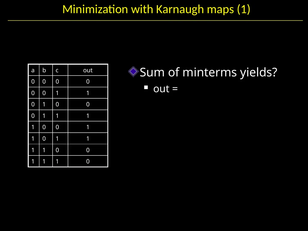
slide29. Sum of minterms yields?
out = Minimization with Karnaugh maps (1)<br>
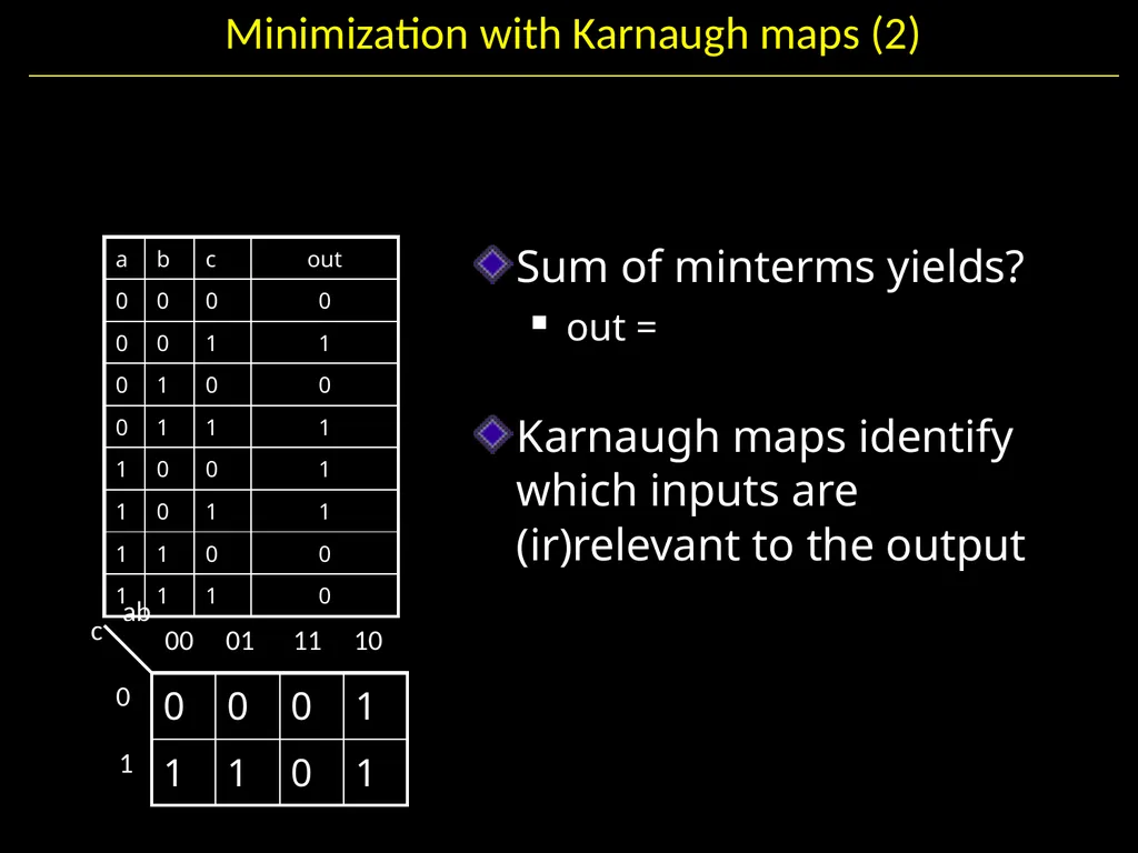
slide30. Sum of minterms yields?
out =
Karnaugh maps identify which inputs are (ir)relevant to the output 00 01 11 10 0 1 c ab Minimization with Karnaugh maps (2)<br>
slide31. Sum of minterms yields?
out =
Karnaugh map minimization
Cover all 1’s
Group adjacent blocks of 2n 1’s that yield a rectangular shape
Encode the common features of the rectangle
out = ab + ac 00 01 11 10 0 1 c ab Minimization with Karnaugh maps (2)<br>
slide32. Karnaugh Minimization Tricks (1) Minterms can overlap
out =
Minterms can span 2, 4, 8 or more cells
out = 00 01 11 10 0 1 c ab 00 01 11 10 0 1 c ab<br>
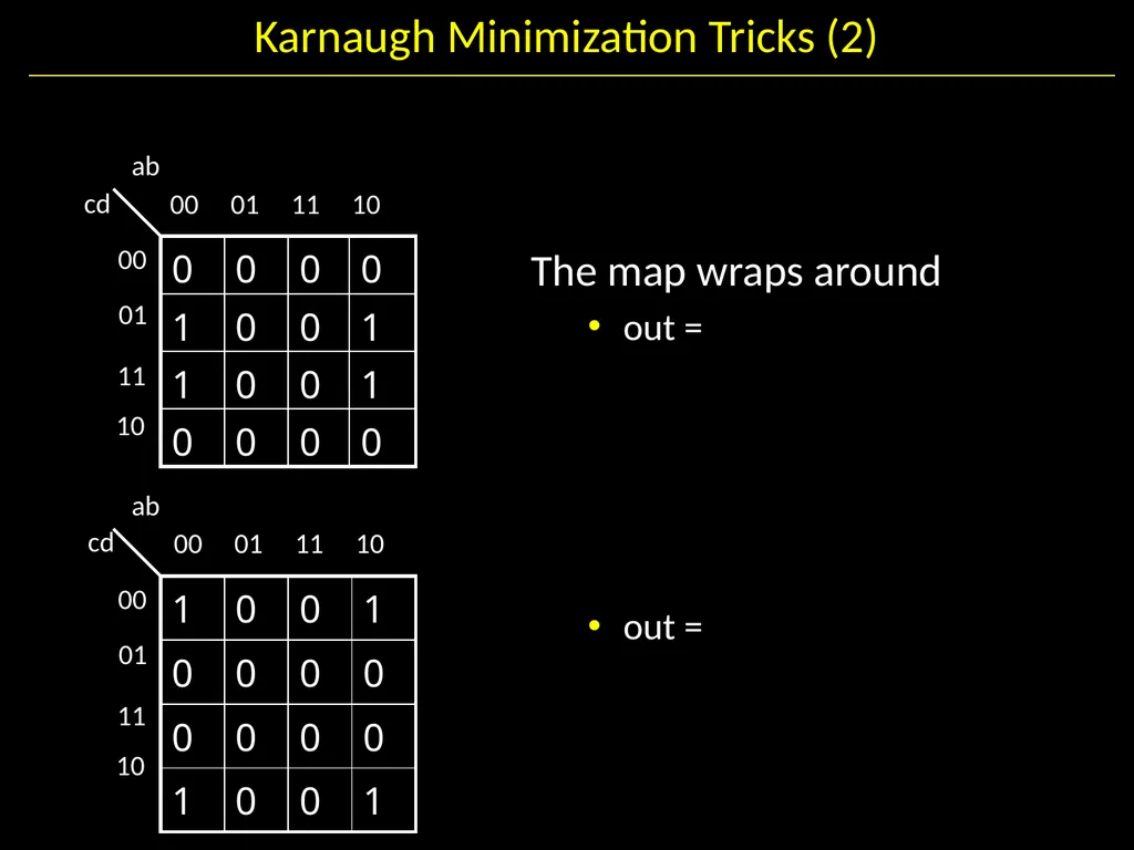
slide33. Karnaugh Minimization Tricks (2) The map wraps around
out =
out = 00 01 11 10 00 01 ab cd 11 10 00 01 11 10 00 01 ab cd 11 10<br>
slide34. Karnaugh Minimization Tricks (3) “Don’t care” values can be interpreted individually in whatever way is convenient
assume all x’s = 1
out =
assume middle x’s = 0
assume 4th column x = 1
out = 00 01 11 10 00 01 ab cd 11 10 00 01 11 10 00 01 ab cd 11 10<br>
slide35. Multiplexer A multiplexer selects between multiple inputs
out = a, if d = 0
out = b, if d = 1
Build truth table
Minimize diagram
Derive logic diagram<br>
slide36. Takeaway Binary (two symbols: true and false) is the basis of Logic Design
More than one Logic Circuit can implement same Logic function. Use Algebra (Identities) or Truth Tables to show equivalence.
Any logic function can be implemented as “sum of products”. Karnaugh Maps minimize number of gates.<br>
slide37. Goals for Today From Transistors to Gates to Logic Circuits
Logic Gates
From transistors
Truth Tables
Logic Circuits
Identity Laws
From Truth Tables to Circuits (Sum of Products)
Logic Circuit Minimization
Algebraic Manipulations
Truth Tables (Karnaugh Maps)
Transistors (electronic switch)<br>
slide38. NMOS Transistor
Connect source to drain when VG = Vsupply
N-channel transistor VS = 0 V VG VG = VSupply VG = 0 V NMOS and PMOS Transistors PMOS Transistor
Connect source to drain when VG = 0 V
P-channel transistor VG VG = VSupply VG = 0 V VD VD = 0V Closed switch
When VG = Vsupply Closed switch
When VG = 0 V Vsupply VS = Vsupply Vsupply Vsupply VD VD = Vsupply<br>
slide39. NMOS Transistor
Connect source to drain when gate = 1
N-channel transistor D S = 0V G G = 1 G = 0 NMOS and PMOS Transistors PMOS Transistor
Connect source to drain when gate = 0
P-channel transistor Vsupply D G G = 1 G = 0 D = 0 Closed switch
When VG = Vsupply Closed switch
When VG = 0 V S = Vsupply Vsupply Vsupply D = 1<br>
slide40. Inverter Function: NOT
Called an inverter
Symbol:
Useful for taking the inverse of an input
CMOS: complementary-symmetry metal–oxide–semiconductor in out Truth table A out Vdd = hi Vss = gnd A = 0<br>
slide41. NAND Gate Function: NAND
Symbol: b a out A out Vdd B B A Vdd Vss<br>
slide42. NOR Gate A out Vss Vdd B B A Vss b a out Function: NOR
Symbol:<br>
slide43. Building Functions (Revisited) NOT:
AND:
OR:
NAND and NOR are universal
Can implement any function with NAND or just NOR gates
useful for manufacturing<br>
slide44. Building Functions (Revisited) NOT:
AND:
OR:
NAND and NOR are universal
Can implement any function with NAND or just NOR gates
useful for manufacturing b a b a a<br>
slide45. Logic Gates One can buy gates separately
ex. 74xxx series of integrated circuits
cost ~$1 per chip, mostly for packaging and testing
Cumbersome, but possible to build devices using gates put together manually<br>
slide46. Then and Now The first transistor
on a workbench at
AT&T Bell Labs in 1947
Bardeen, Brattain, and Shockley An Intel Westmere
1.17 billion transistors
240 square millimeters
Six processing cores http://www.theregister.co.uk/2010/02/03/intel_westmere_ep_preview/<br>
slide47. Summary Most modern devices are made from billions of on /off switches called transistors
We will build a processor in this course!
Transistors made from semiconductor materials:
MOSFET – Metal Oxide Semiconductor Field Effect Transistor
NMOS, PMOS – Negative MOS and Positive MOS
CMOS – Complimentary MOS made from PMOS and NMOS transistors
Transistors used to make logic gates and logic circuits
We can now implement any logic circuit
Can do it efficiently, using Karnaugh maps to find the minimal terms required
Can use either NAND or NOR gates to implement the logic circuit
Can use P- and N-transistors to implement NAND or NOR gates<br>
slide48. Big Picture: Abstraction Hide complexity through simple abstractions
Simplicity
Box diagram represents inputs and outputs
Complexity
Hides underlying P- and N-transistors and atomic interactions<br>