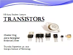
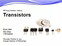
Transistors Ryan Akin Xin Chen Will Dahlin Thursday October 6 2011 Georgia Institute of Technology Introduction to Transistors Ryan Akin Field Effect and Power Transistors Will Dahlin ID: 162429
Download Presentation The PPT/PDF document "ME 6405 Student Lecture:" is the property of its rightful owner. Permission is granted to download and print the materials on this web site for personal, non-commercial use only, and to display it on your personal computer provided you do not modify the materials and that you retain all copyright notices contained in the materials. By downloading content from our website, you accept the terms of this agreement.
Slide1
ME 6405 Student Lecture:Transistors
Ryan Akin
Xin ChenWill Dahlin
Thursday October 6, 2011
Georgia
Institute of TechnologySlide2
Introduction to Transistors
Ryan Akin
Field Effect and Power Transistors
Will
Dahlin
1
3
4
Transistor Part Numbers and Catalog
Will Dahlin
5
Bipolar Junction TransistorsXin Chen
2
Presentation Outline
Transistor Types and Checks
Ryan AkinSlide3
Definition & Fundamental Need
Brief History
Transistor Role in Modern ElectronicsTwo Basic Transistor FunctionsDoping process and its effects on function
Introduction to TransistorsSlide4
Transistors
First Transistor
Model, 1947FET Transistor
BJT Transistor
Transistors of various type & size
Used in all modern electronics
BJT (PNP) Electrical Diagram RepresentationSlide5
tran·sis·tora semiconductor device that amplifies, oscillates, or switches the flow of current between two terminals by varying the current or voltage between one of the terminals and a third. (www.dictionary.com)
www.coltecnica.comSlide6
Basic Purpose [1] To electronically switch (no moving parts) a signal on or off (high/low) [2] To amplify signalsRole in Modern Electronics
Basic building blocks for all modern electronicsMicroprocessors, Microcontrollers, Computers, Digital watches, Digital Logic Circuits, Cell Phones….
Microprocessor
PC & Cell Phones
Motor Controllers
HeadphonesSlide7
Early 20th century, vacuum tube were used as signal amplifiers & switches.
U
se of vacuum tube* resulted in extremely large, fragile, energy inefficient, and expensive electronics.Evolution of electronics required device that was small, light weight, robust, reliable, cheap to manufacture, energy efficient… *Vacuum tube advantages: operation at higher voltages (10K region vs. 1K region of transistors); high power, high frequency operation (over-the-air TV broadcasting) better suited for vacuum tubes; and silicon transistors more vulnerable to electromagnetic pulses than vacuum tubes
Reason for Transistor’s Invention:
Vacuum Tube Radios
ENIAC : 17, 468 vacuum tubesSlide8
InventionIn 1947, John Bardeen, Walter Brattain, and William Schockly, researchers at Bell Lab, invented Transistor.They found Transistor Effect: “when electrical contacts were applied to a crystal of germanium, the output power was larger than the input.”Awarded the Nobel Prize in physics (1956)Revolutionized portability and efficiency of electronic devices
John Bardeen, Walter Brattain, and William
SchocklyFirst model of Transistor, 1947Slide9
Infinite possibilities
V
ground
mVSlide10
Transistor Manufacturing Process
Doping:
“Process of introducing impure elements (dopants) into semiconductor wafers to form regions of differing electrical conductivity.”Doping impurities into a “pure”semiconductor will increase conductivity.Doping results in an “N-Type” or “P-Type” semiconductor.
Ion Implanter
Wafer
Refinement
High-Temp Furnace“Pure” Wafers“Doped” WafersSlide11
Effect of Doping on Semi-Conductors
P-Type Semiconductors : Positively charged SemiconductorDopant Material:
Boron, Aluminum, GalliumEffect of Dopant: Creates “holes” (positive charges where electrons have been removed) in lattice structureSlide12
Effect of Doping on Semi-Conductors
N-Type Semiconductors : Negatively charged SemiconductorDopant Material:
Phosphorous, Arsenic, Antimony (Sb)Effect of Dopant: Added unbound electrons create negative charge in lattice structure Remember: Dopant is added to same piece of semiconductor materialResulting Material: Single, solid material called “P-N Junction”Slide13
Electrical Switching on P-N Junction
Applying External Voltage……of Forward Biasing
polarity facilitates motion of free electrons…of Reverse Biasing polarity impedes motion of free electrons
Reverse Biasing
Forward Biasing
Circuit is “Off”Current not Flowing
Circuit is “On”Current is FlowingSlide14
Finally – combining all concepts
Semiconductor -> Doping -> P-N Junction -> Depletion RegionOne P-N Junction can
control current flow via an external voltageTwo P-N junctions (bipolar junction transistor, BJT) can control current flow and amplify the current flow. Also, if a resistor is attached to the output, the resulting voltage output is much greater than the applied voltage, due to amplified current. Example at end.
Slide15
http://www.youtube.com/watch?v=QO5FgM7MLGg Slide16
Introduction to Transistors
Ryan Akin
Field Effect and Power Transistors
Will
Dahlin
3
4
Transistor Part Numbers and Catalog
Will
Dahlin5
Bipolar Junction Transistors
Xin Chen
1Presentation Outline
Transistor Types and Checks
Ryan Akin
2Slide17
Types and Categorization of Transistors
Meter Check of Unknown Transistor
Transistor Types and ChecksSlide18
Transistor are categorized bySemiconductor material: germanium, silicon, gallium arsenide, etc. Structure: BJT, FET, IGFET (MOSFET), IGBT
Polarity: NPN, PNP (BJTs); N-channel, P-channel (FETs)
Maximum power rating: low, medium, high Maximum operating frequency: low, medium, high Application: switch, audio, high voltage, etc. Physical packaging: through hole, surface mount, ball grid array, etc.Amplification factor, βVarious Types of Transistor: http://en.wikipedia.org/wiki/Category:Transistor_types
Various Types of Transistors
Bipolar Junction Transistor (BJT)
Field Effect Transistors (FET)Power TransistorsTransistor Categories and TypesSlide19
Meter check of a transistorBipolar transistors are constructed of a three-layer semiconductor “sandwich,” either PNP or NPN. As such, transistors register as two diodes connected back-to-back when tested with a multimeter's “resistance” or “diode check” functionSlide20
For PNP Transistors1. Set multimeter to Ohmmeter Ohm Scale. 2. Connect the Negative Probe (Black) to Emitter and the Positive Probe (Red) to the Base(R=R1).3. Now invert the probe connections to the Emitter for the Red Probe and to the Base for Black. R = “OL”.
If this works, your Emitter-Base junction is OK. 4. Now test the Base-Collector junction. Connect the Red probe to the Base and the Black probe to the
Collector (R=R2).5. Invert the probes again, Black to the Base and the Red probe to the Collector. R = “OL”.If this works, your Base-Collector junction is Ok. 6. Connect the probes to the Emitter and Collector (probes may be inverted), R = “OL”indicates a working transistor.Meter check of a transistorSlide21
For NPN Transistors1. Set multimeter to Ohmmeter Ohm Scale.2. Connect the Negative Probe (Black) to Base and the Positive Probe (Red) to the Emitter.(R=R 1).3. Now invert the probe connections to the Base for the Red Probe and to the Emitter for Black. R = “OL”.
If this works, then your Emitter-Base junction is OK. 4. Now test the Base-Collector junction. Connect the Black probe to the Base and the Red probe to the Collector(R=R 2).
5. Invert the probes again, Red to the Base and the Black probe to the Collector. R = “OL”.If this works, then your Base-Collector junction is Ok. 6. Connect the probes to the Emitter and Collector (probes may be inverted), R “OL” indicates a working transistor.Meter check of a transistorSlide22
Detecting defective Transistors1. If their is no resistance between any of the pairs during test (R = 0) for all the steps, then the transistor is shorted. 2. If for all the steps R = “OL”, then the transistor is open.“OL” – resistance is greater than the meter can read
Meter check of a transistorSlide23
Introduction to Transistors
Ryan Akin
Field Effect and Power Transistors
Will
Dahlin
4
Transistor Part Numbers and Catalog
Will Dahlin
5
Bipolar Junction TransistorsXin
Chen
1Presentation Outline
Transistor Types and ChecksRyan Akin
3
2Slide24
BJT introductionBJT =
Bipolar Junction T
ransistorA BJT consists of two back-to-back p-n junctions. The three regions are the emitter(E),base(B),and collector(C).The middle region, the base is very thin. Since the base is thin, most carriers from emitter injected into base diffuse into collector.Slide25
NPN
PNP
NPN: BE forward biasedBC reverse biasedPNP: BE reverse biased
BC forward biased
BJT schematicSlide26
BJT Transistor Operationhttp://www.learnabout-electronics.org/bipolar_junction_transistors_05.phpSlide27
BJT formulae
NPN
Current controlβ is the amplification factor and ranges from 20 to 200It is dependent on temperature and voltageSlide28
BJT formulaeNPN
Emitter is more heavily doped than the collector.
Therefore, VC > VB > VEfor NPN transistorSlide29
BJT formulaeNPN
α
is the fraction of electrons that diffuse across the narrow base region1 – α is the fraction of electrons that
recombine with holes
in the base region to create base currentSlide30
BJT Characteristic CurvesTransfer CharacteristicThe graph of I
CE / IBE shown (right) is called the Transfer Characteristic
The slope of the graph shows the β Characteristic curves (graphs) can be drawn to show other parameters of a transistor, and are used both to detail the performance of a particular device and as an aid to the design of amplifiers.Slide31
Input CharacteristicBJT Characteristic Curves
The Input Characteristic is the base emitter current IBE against base emitter voltage V
BE(IBE/VBE) shows the input Conductance of the transistor.The steepness of this particular curve when the VBE is above 1 volt shows that the input conductance is very high, and there is a large increase in current (in practice, usually enough to destroy the transistor!) for a very small increase in VBE.Therefore the input RESISTANCE must be low. Slide32
BJT Characteristic CurvesOutput Characteristic
The slope gives the value of output conductance (and by implication output resistance).
The near horizontal parts of the graph lines show that a change in collector emitter voltage VCE has almost no effect on collector current in this region, just the effect to be expected if the transistor output had a large value resistor in series with it.Therefore the graph shows that the output resistance of the transistor is high.Slide33
BJT operating regions
Operating Region
ParametersMode
Cut Off
V
BE
< Vcut-in VCE
> VsupplyIB = IC
= 0Switch OFFLinear
VBE = Vcut-in
Vsat < VCE < Vsupply
IC = β*IB
AmplificationSaturated
VBE
=
V
cut
-in
,
V
CE
<
V
sat
I
B
>
I
C,max
,
I
C,max
> 0
Switch ONSlide34
The Transistor as A SwitchWhile there are limitations as to what we can switch on and off, transistor switches offer lower cost and substantial reliability over conventional mechanical relays.
The secret to making a transistor switch work properly is to get the transistor in a saturation stateSlide35
From
exercise 3
Turns on/off coils digitally
The Transistor as A AmplifierSlide36
The Transistor as A AmplifierTransistor ConnectionsBecause an amplifier must have two input and two output terminals, a transistor used as an amplifier must have one of its three terminals common to both input and output as shown on the right. The choice of which terminal is used as the common connection has a marked effect on the performance of the amplifier.
There are three connection modes:
Comm0n Emitter ModeCommon Collector ModeCommon Base ModeSlide37
The Transistor as A Amplifier
Parameter
Common EmitterCommon CollectorCommon BaseVoltage gain AvHigh (about 100)Unity (1)Medium (10-50)Current GainHigh (50 - 800)High (50 -800)Less than unity (<1)Input Impedance
Medium (about 3 to 5k)
High (several k)
Low (about 50R)Output ImpedanceMedium, Approx = Load resistor valueLow (a few ohms)High (about 1M)Summary of the three types transistor connectionSlide38
Several Comments about TransistorBipolar transistor consists of two PN junctions, with two types: NPN and PNP BJT is a current control device.
The ratio of currents leads to one of the most important parameters of a transistor, which is its “current gain”, often referred to as its “Beta”.
BJT itself does not generate extra energy for amplifying, it just uses small current change to control big current change, which comes from the power supply.Slide39
The Common Emitter Amplifier NPN Transistor - Both the signal source and the load share the emitter lead as a common connection point - The common emitter configuration lends itself to voltage amplification and is the most common configuration for transistor amplifiers.
Slide40
The Common Emitter Amplifier
The capacitor C1 must be used t0 keep
any DC component from disturbing the carefully developed biasing which establishes the operating point But C1 also puts a High-Pass Filter on theInput and must be chosen so that it does not filter out the lowest frequency which is to be amplified Likewise, the capacitor C2 provides DC blocking and must be prevented from attenuating the signalSlide41
The Common Emitter Amplifier Resistors R1 and R2 are used to properly bias the transistor to keep it working in the active region
These resistors are used as a voltage divider to provide proper value of base voltage to fit the chosen operating point.For reasonable stability, usually make the current through these resistors at least 10 times of the base current.
In the range of active operation of the TransistorThe base voltage is
The voltage divider requirement is
Slide42
The Common Emitter Amplifier The resistance RC + RE determines the maximum collector current
The capacitor C
E bypasses the emitter resistor RE, making it an AC ground.The reason is that a rise in signal would increase the current through the resistor and therefore the voltage at the emitter.Slide43
The Common Emitter Amplifier NPN Transistor - Both the signal source and the load share the emitter lead as a common connection point - The common emitter configuration lends itself to voltage amplification and is the most common configuration for transistor amplifiers.
Slide44
NPN TransistorThe Common Collector Amplifier The common collector amplifier, often called an emitter follower since its output is taken from the emitter resistor, is useful as an impedance matching device since its input impedance is much higher than its output impedance. It is also termed a "buffer" for this reason and is used in digital circuits with basic gates.Slide45
Emitter Follower DiscussionThe Common Collector Amplifier The voltage gain of an emitter follower is just a little less than one since the emitter voltage is constrained at the diode drop of about 0.6 volts below the base . Its function is not voltage gain but current or power gain and impedance matching. It's input impedance is much higher than its output impedance so that a signal source does not have to work so hard. This can be seen from the fact that the base current in on the order of 100 times less that the emitter current. The low output impedance of the emitter follower matches a low impedance load and buffers the signal source from that low impedanceSlide46
NPN Transistor The Common Base Amplifier This configuration is used for high frequency applications because the base separates the input and output, minimizing oscillations at high frequency. It has a high voltage gain, relatively low input impedance and high output impedance compared to the common collector.Slide47
Introduction to Transistors
Ryan Akin
Field Effect and Power Transistors
Will Dahlin
3
Transistor Part Numbers and Catalog
Will Dahlin
5
Bipolar Junction
TransistorsXin Chen
1
Presentation Outline
Transistor Types and ChecksRyan Akin
4
2Slide48
Power TransistorsConcerned with delivering high power Used in high voltage and high current application
In generalFabrication process different in order to:
Dissipate more heatAvoid breakdownDifferent types: Power BJTs, power MOSFETS, etc.Slide49
Field-Effect Transistor (FET)Slide50
What makes a Field-Effect Transistor? FETs have three main parts
Drain Source
GateThe body has contacts at the ends: the drain and sourceGate surrounds the body and can induce a channel by use of an electric fieldFETBJT
Input
voltage controls output current
Input current controls output currentGate
BaseControls flow of currentDrainCollector
Current goes out hereSourceEmitterCurrent comes in hereSlide51
What is a Field-Effect Transistor (FET)? Semiconductor device that depends on electric field to control the current
Performs same functions as a BJT; amplifier, switch, etc.
Relies on PNP or NPN junctions to allow current flow However, mechanism that controls current is different from the BJT Remember the BJT is bipolar. The FET is sometimes called a unipolar
transistor
One type of charge carrierSlide52
How does a FET work?
Flow of current is similar to water flow through a garden hose
Pinch the hose (decrease current channel width) to decrease flow
Open the hose (increase channel width) to increase flow
Also, the pressure differential from the front and back of the hose (synonymous with the voltage from drain to source) effects the flow
JFET AnimationSlide53
Types of Field-Effect Transistors
MOSFET
IGBTTypeFunction
J
unction Field-Effect Transistor (JFET)Uses reversed biased p-n junction to separate gate from body
Metal-Oxide-Semiconductor FET (MOSFET)
Uses insulator (usu. SiO2) between gate and body Insulated Gate Bipolar Transistor (IGBT)
Similar to MOSFET, but different main channel Organic Field-Effect Transistor (OFET)
Uses organic semiconductor in its channel Nanoparticle Organic Memory FET (NOMFET)
Combines the organic transistor and gold nanoparticlesSlide54
JFETA single channel of single doped SC material with terminals at endGate surrounds channel with doping that is opposite of the channel, making the PNP or NPN typeUses reversed biased p-n junction to separate gate from body
n-channel
JFETp-channelJFETSlide55
Characteristics and Applications of FETsJFETs
Simplest type of FET – easy to make
High input impedance and resistanceLow CapacitanceSlower speed in switchingUses?Displacement sensorHigh input impedance amplifierLow-noise amplifierAnalog switchVoltage controlled resistorSlide56
MOSFETSimilar to JFET A single channel of single doped SC material with terminals at endGate surrounds channel with doping that is opposite of the channel, making the PNP or NPN typeBUT, the MOSFET uses an insulator to separate gate from body, while JFET uses a reverse-bias p-n junction
p-channel
n-channelMOSFET
enhanced mode
MOSFET
depleted modeSlide57
How does a MOSFET work?
Simplified Notation
No current flow“Short” allows current flowNo Voltage to Gate
Voltage to Gate
Source
SourceDrainDrain
nnSlide58
MOSFETFETs vary voltage to control current. This illustrates how that works
MOSFET drain current vs. drain-to-source voltage for several values of
VGS − Vth; the boundary between linear (Ohmic) and saturation (active) modes is indicated by the upward curving parabola.Slide59
MOSFET
Triode Mode/Linear Region
VGS > Vth and VDS < ( VGS - Vth )VGS : Voltage at the gateV
th
: Threshold voltage
VDS : Voltage from drain to sourceμn: charge-carrier effective mobilityW: gate width L: gate length Cox : gate oxide capacitance per unit areaλ : channel-length modulation parameterSaturation/Active Mode VGS > V
th and VDS > ( VGS - Vth )Slide60
Characteristics and Applications of FETsMOSFETs
Oxide layer prevents DC current from flowing through gate
Reduces power consumptionHigh input impedanceRapid switchingMore noise than JFETUses?Again, switches and amplifiers in generalThe MOSFET is used in digital CMOS logic, which uses p- and n-channel MOSFETs as building blocksTo aid in negating effects that cause discharge of batteriesUse of MOSFET in battery
protection circuitSlide61
Introduction to Transistors
Ryan Akin
Field Effect and Power Transistors
Will Dahlin
3
Transistor Part Numbers and Catalog
Will Dahlin
4
Bipolar Junction
TransistorsXin
Chen
1Presentation Outline
Transistor Types and ChecksRyan Akin
5
2Slide62
How to choose and appropriate transistor
Reading part numbers
Numerous “Standards” – JIS, JEDEC, Pro Electron, etc.Dependent on manufacturer and customer
Transistor Catalog
ZTX 652/653 Datasheet
If in doubt, meter checkTransistor Part Numbers and CatalogSlide63
Introduction to Transistors
Ryan Akin
1
Bipolar Junction
Transistors
Xin
Chen3
Presentation Summary
Introduction & FormulaeExplain function and characteristics of common emitter transistorDescribe BJT operating regionsApplications of BJTs
Qualitative explanation of the what & how behind transistorsGeneral application and history of transistors“Physics” behind transistors : Doping Process, Effect on Semiconductors, & Formation of P-N Junction Electrical Properties of P-N Junction & using P-N to control / amplify current
Transistor Types and Checks Ryan Akin
2
Categorized by type, ratings, structure
Meter check of unknown transistorSlide64
Field Effect and Power Transistors
Will Dahlin
Transistor Part Numbers and Catalog
Will Dahlin
4
5
Presentation Summary
Definition and Applications
Use of electric field to change the output current JFETs and MOSFETs are most common, and accomplish similar goals as BJTs Used for switches, amplification, applications for protecting electronics
Part numbers can be arbitraryTransistor Catalog and DatasheetSlide65
Example Problem – Ryan AkinSlide66
Referenceshttp://www.utdallas.edu/research/cleanroom/TystarFurnace.htm
http://www.osha.gov/SLTC/semiconductors/definitions.htmlhttp://www.products.cvdequipment.com/applications/diffusion/1/
http://amath.colorado.edu/index.php?page=an-immersed-interface-method-for-modeling-semiconductor-deviceshttp://www.extremetech.com/article2/0,2845,1938467,00.asphttp://macao.communications.museum/eng/Exhibition/secondfloor/moreinfo/2_10_3_HowTransistorWorks.htmlhttp://fourier.eng.hmc.edu/e84/lectures/ch4/node3.htmlhttp://www.appliedmaterials.com/htmat/animated.html http://hyperphysics.phy-astr.gsu.edu/hbase/solids/dope.html#c3http://www.tpub.com/neets/book7/25.htmhttp://esminfo.prenhall.com/engineering/wakerlyinfo/samples/BJT.pdfhttp://web.engr.oregonstate.edu/~traylor/ece112/lectures/bjt_reg_of_op.pdfhttp://www.me.gatech.edu/mechatronics_course/transistors_F09.ppt
http://en.wikipedia.org/wiki/Bipolar_junction_transistor
http://en.wikipedia.org/wiki/Common_emitter
http://en.wikipedia.org/wiki/Diodehttp://www.kpsec.freeuk.com/trancirc.htmhttp://en.wikipedia.org/wiki/Field-effect_transistorhttp://en.wikipedia.org/wiki/JFEThttp://en.wikipedia.org/wiki/MOSFEThttp://www.slideshare.net/guest3b5d8a/fetshttp://www.rhopointcomponents.com/images/jfetapps.pdfhttp://cnx.org/content/m1030/latest/http://www.play-hookey.com/semiconductors/enhancement_mode_mosfet.html
http://www.youtube.com/watch?v=-aHnmHwa_6I&feature=relatedhttp://www.youtube.com/watch?v=v7J_snw0Eng&feature=relatedhttp://info.tuwien.ac.at/theochem/si-srtio3_interface/si-srtio3.htmlhttp://hyperphysics.phy-astr.gsu.edu/hbase/solids/dope.html#c4http://inventors.about.com/library/inventors/blsolar5.htmhttp://thalia.spec.gmu.edu/~pparis/classes/notes_101/node100.htmlhttp://hyperphysics.phy-astr.gsu.edu/hbase/solids/pnjun.html#c3http://science.jrank.org/pages/6925/Transistor.html really good explanation!http://www.learnabout-electronics.org/fet_01.phphttp://www.learnabout-electronics.org/bipolar_junction_transistors_01.phpSlide67
Questions?
Thank you!