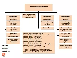
Presented at Seoul Korea April 19 2011 APEC Green Innovation Conference Korea Success Story JUSUNG Served Markets in Solar Low Cost aSi Thin Film for Large Scale Utility High Efficiency Crystalline Silicon ID: 276620
Download Presentation The PPT/PDF document "Y.G Lee, Executive Vice President" is the property of its rightful owner. Permission is granted to download and print the materials on this web site for personal, non-commercial use only, and to display it on your personal computer provided you do not modify the materials and that you retain all copyright notices contained in the materials. By downloading content from our website, you accept the terms of this agreement.
Slide1
Y.G Lee, Executive Vice PresidentPresented at Seoul, KoreaApril 19, 2011
APEC Green Innovation Conference
Korea Success StorySlide2
JUSUNG Served Markets in Solar
Low Cost a-Si Thin Film
for Large Scale Utility
High Efficiency Crystalline Silicon
for Rooftops
Transparent PV with Higher Output
for Building Integration
JUSUNG is a Leading Solar Technology and Production Equipment Solutions Partner Slide3
Solar Market Forecasts
Analysts May Have Different Viewpoints on the Market – “Sunny Future for Solar” or “Cloudy Days”…
…Though All Forecasters Universally Agree that
Solar Will Grow…Slide4
The Photovoltaic LandscapeAttributes
Cells/Modules
Technology
Thin Film
Absorber & Conductive Materials Deposited on Glass Sheets
a
-Si (Single/Tandem),
CdTe
, CIGS, See-Thru BIPV
Crystalline Silicon
Processing Silicon Wafers into Solar Cells
Multi-, Mono-, Selective Emitter,
Heterojunction
Widely Used Conventional Technology
High “Name Plate” Conversion Efficiency, 16%-22%
Lighter Weight
Lower Capital Expenditures, Higher Running Costs, i.e., Polysilicon
Applications: Residential and Commercial Rooftops, Ground Mount Solar Farms
“New” (But Old) Technology
Lowest Production Costs, < US$0.80
Modest Conversion Efficiencies, 8%-12%
Less Affected from Shading and Temperature Effects
No Raw Materials Constraints
Applications: Ground Mount Solar Farms, Commercial Rooftops, Building GlassSlide5
Solar Value ChainCrystalline Silicon
Thin Film
JUSUNG Products
Plasma Enhanced Chemical Vapor Deposition Systems for
Passivation
, Anti-Reflective and Absorber Layers
Reactive Ion Etchers for
Texturization
Physical Vapor Deposition Systems Conductive Films
Turnkey Factories for
Heterojunction
Technology
Glass
PV Cell/Module
System
JUSUNG Products
Plasma Enhanced Chemical Vapor Deposition Systems for Absorber Layers
Metal Organic Chemical Vapor Deposition Systems for Transparent Conductive Coatings
Physical Vapor Deposition Systems Conductive Films
Turnkey FactoriesSlide6
JUSUNG Customer Value Proposition
JUSUNG provides capital efficient, enabling technology solutions through World-Class innovation and partnership. Our products and services create value to our customers by helping them achieve market leadership as the World’s #1 in cost, productivity, and profitability.Slide7
JUSUNG at a Glance Korea’s Largest Manufacturer of Capital Equipment for Semiconductors, Solar, LED, and Flat Panel DisplaysFounded in 1995Headquarters: Gyeonggi
-Do (Seoul Area), South Korea
Listed on KOSDAQ in 1999, Ticker Symbol 036930
Global Sales and Service Offices in United States, China, Taiwan, Japan, and Europe
Strong Track Record with Large Customers –
Hynix
, LG Display, Texas Instruments, IBM, TSMC, and more
2010 Revenues > KRW423bn
,
150% YoY
growth, extending into 2011Profitable and GrowingSlide8
Bn KRW
‘95
‘97
‘98
‘99
‘00
‘01
‘02
‘03
‘04
‘05
‘06
‘96
’07
’08
’09
History of Product Innovation Leads to Growth
’10
’11 est
Increasing Products and Adjacent Served Markets Drive Company GrowthSlide9
Jusung Business Segmentation 2006-2010
Regional
Revenue
(Wbn) : 121.1 212.0 152.2 170.1 423.4
3%
Korea Taiwan China EU USA
Products
Revenue
(Wbn)
:
121.1 212.0 152.2 170.1 423.4
Solar Cell FPD/OLED Semiconductor/LED
Solar is the Largest Segment for Jusung Business >2010Slide10
1995~
Semiconductor
Equipment
Diffusion
Thin Films
Etch
2002~
Display
Equipment
TFT-LCD
OLED
Leveraging Production Proven Platforms
JUSUNG’s Technology DNA in Solar Products
2006~
Solar Cell
Total Solution
Thin Film Si
Crystalline Si
Providing Enabling, Cost Effective, and Manufacturable Solutions to Solar
Materials Science of Thin Film Deposition and Etch
“Moore’s Law” for Technology Innovation
Vacuum and Plasma Physics for Precise Processing
Large Area Processing Expertise
Scaling Capability
Low Cost Manufacturing MentalitySlide11
Case Study of JUSUNG Product Developmentc-Si Solar
FPD Gen 6 (2001)
Solar Soultera PECVD Gen 6 (2008)
Semiconductor PECVD (2000)
Utilizing Common Platforms Shortens Time to Market, Decreases Execution Risk, and Increases Operational Leverage
Use Flat Panel Display Product as Backbone
Production Proven with >300 Units Shipped Since 2001
Add Know-How of Semiconductors
Thin Film Process Control
Resulting in Industry Leading Productivity
>2800 Wafers/Hour
Improved Cell Efficiency, >0.5%
Highest Uptime, >95%Slide12
Individual Systems to Turnkey FactoriesBest of Breed Systems are Building Blocks to Turnkey Factories That Proliferates Capital Efficient Solar Manufacturing
Top PECVD
Bottom PECVD
Laser Scriber P4
Module Sorter
Sputter
AOI
Cleaner
Back Glass Loader
Front Glass Loader
Laminator
Simulator
Cleaner
Cleaner
Lay-UP
Simulator
RMS
ID Marker
Dry Cleaner
Glass
I
n
Glass Out
Laser Scriber P3
Laser Scriber P2
Laser Scriber P1
Sand Blaster
300MW Thin Film Turnkey Factory
World’s Best Cost and Performance
$0.59/
Wp
Cost of Ownership
>10.2% Stabilized Efficiency
Front MOCVD
PECVD Absorber Deposition System
PVD Metallization System
TCO Deposition SystemSlide13
JUSUNG Worldwide Headquarters in KoreaInvesting in Capacity to Meet Increasing Market Opportunities
Solar C-Si
R&D
BIPV R&D
OLED R&D
LCD & Solar TF R&D
Manufacturing Facility 1
SEMI & LED R&D
Manufacturing Facility 2
Standardization R&DSlide14
Investment in In-House Pilot LinesFully Equipped Pilot Lines for Thin Film and c-Si Device IntegrationSlide15
Intellectual Property is Our PriorityHighest Level of Intellectual Property Generates Unique & Innovative Technologies
JUSUNG IP includes Korea and international IPs listed globally. Sources:
www.wips.co.kr
, government patent offices, company webpages.Slide16
Human Resources Stability Allows for Consistent High Performance…Regardless of Business CyclesHuman Resources are a Strategic AssetSlide17
JUSUNG’s Global Infrastructure41 Customers in the World
4 Subsidiaries, 14 Offices, 5 Sales Agents for Global Support
HQ
◆
◆
◆
◆
◆
Korea
8 Customers
Japan
3 Customers
Europe
6 Customers
China
6 Customers
USA
7 Customers
Singapore
1 Customer
Philippines
1 Customer
Malaysia
1 Customer
Headquarter
Subsidiary
Local Office
Sales Agent
Taiwan
8 Customer
Solar is Global…as is JUSUNG’s FootprintSlide18
Solar Megatrends and JUSUNG’s PreparationAverage Selling Prices Will Continue to Decline Until Grid ParityFeed-in Tariffs and Subsidies Reduction Forces Industry to Evolve into Self Sufficiency Through Cost RoadmapsJUSUNG’s Solutions: Capital Efficient Technologies – Higher Throughput, Uptime, and Conversion Efficiencies
Many Companies Have Reach Manufacturing Efficiencies of Scale for Cost Reduction
Seeking Technology for Efficiency Gains to Further Cost Roadmap
JUSUNG’s Solutions:
Uniquely Differentiated Products
in c-Si PECVD, Reactive Ion Etcher, Heterojunction, Thin Film
Manufacturing is Concentrating in Asia
Favorable Government Partnerships and Lower Cost of Manufacturing
JUSUNG’s Solutions:
Strategically Located in Asia, with >100 Service Engineers for Mainland China, Malaysia, Philippines, Taiwan China, and KoreaSlide19
Key Takeaways from the JUSUNG StoryEstablished HQ and Global Infrastructure for Customer Engagements
Investing in R&D, Production Capacity, Human Capital
Production Proven in Semiconductors and
Flat Panel Display
Innovative Technologies, Unique ProductsSlide20
Innovation beyond the limit.Thank You
Joe Feng
joe_feng@jseng.com