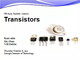
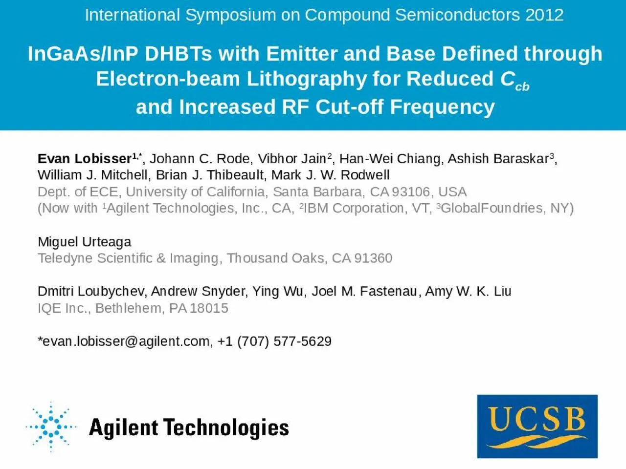
PPT-InGaAs/InP DHBTs with Emitter and Base Defined through Electron-beam

Author : audrey | Published Date : 2024-06-08

Lithography for Reduced C cb and Increased RF Cutoff Frequency Evan Lobisser 1 Johann C Rode Vibhor Jain 2 HanWei Chiang Ashish Baraskar 3 William

Presentation Embed Code

Download Presentation

Download Presentation The PPT/PDF document "InGaAs/InP DHBTs with Emitter and Base D..." is the property of its rightful owner. Permission is granted to download and print the materials on this website for personal, non-commercial use only, and to display it on your personal computer provided you do not modify the materials and that you retain all copyright notices contained in the materials. By downloading content from our website, you accept the terms of this agreement.

InGaAs/InP DHBTs with Emitter and Base Defined through Electron-beam: Transcript


Lithography for Reduced C cb and Increased RF Cutoff Frequency Evan Lobisser 1 Johann C Rode Vibhor Jain 2 HanWei Chiang Ashish Baraskar 3 William J . Paul Roberts CSIRO Australia Telescope National Facility CSIRO Australia Telescope National Facility PaulRoberts PaulRoberts atnf atnf csiro csiro au au 200 180 160 140 120 100 80 60 10000 20000 30000 40000 50000 60000 Voltage mV10 time psec Digitis Transistors. Ryan Akin. Xin. Chen. Will . Dahlin. Thursday October 6, 2011. Georgia. Institute of Technology. Introduction to Transistors. Ryan Akin. Field Effect and Power Transistors. Will . Dahlin. “The most incomprehensible thing about the world is that it is comprehensible.”. – . Albert Einstein. Day. 18, 3/31:. . Questions? . Electron Diffraction. Wave packets and uncertainty. Next Week:. Yue Hao. Collider-Accelerator Department. Brookhaven National Laboratory. Jan 10, 2009 EIC Meeting at Stony Brook. Outline. Beam-beam effect on the Electron beam. Beam distribution disruption. Mismatch with the design lattice. of 200 nm Height by Atomic Layer Epitaxy. *D. Cohen-Elias. 1. , J.J.M. Law. 1. , H.W. Chiang. 1. , A. Sivananthan. 1. , . C. Zhang. 1. , B. J. Thibeault. 1. , W.J. Mitchell. 1. , S. Lee. 1. , A.D. Carter. Identification of transistor type and its . terminals. By:Engr.Irshad. . Rahim. . Memon. OBJECTIVE. Objective of this practical is to identify transistor type such as (. i. ) NPN (ii) PNP,. . and its terminals such as emitter, base and collector.. Qiao Xiang. Advisor: Hongwei Zhang. Outlines. Introduction. In-Network Processing Methods. QoS-Assured INP in WCPS. Open Issues. Conclusion. Outlines. Introduction. In-Network Processing Methods. QoS-Assured INP in WCPS. L.J.Mao. (IMP), . H.Zhang. (. Jlab. ). On behalf of colleagues from . Jlab. , BINP . and . IMP. Motivation. . HIRFL-CSR facility. . Cooling Experiments @ HIRFL-CSR. . Simulation works. Chad . Auginash. April 20, 2015. Abstract. High electron mobility transistor(HEMT) is a transistor that operates at higher frequencies, typically in the microwave range. They are used in applications that require high frequency, such as cell phones, RF applications, and some power applications. HEMTs are transistors that utilize the 2-dimensional electron gas(2DEG) created by a junction between two materials with different band gaps called a heterojunction. The two most commonly used materials to create the heterojunction are a highly doped n-type donor material, typically . [BJT’s]. S.Lakshmanan[ACED]. Basics. Transistor is a solid state Device, whose operation is based on flow of electric charge carriers with in the solid.. Used as Amplification and Switch. It is analogous to a Vacuum triode.. University of Illinois Urbana-Champaign to Install First 150kV Electron Beam Lithography System in North America Contact jcamachocsices Access to provided data and code The provided data set contains a circular scan of the tissue mimicking phantom depicted in Fig 1 based on water gelatin graphite powder and alco due to ISR-induced energy diffusion. Nikolai Yampolsky. Los Alamos National Laboratory. Fermilab. ; February 24, . 2011. FEL principles. S. N. S. N. After one. wiggler period. Radiation slips ahead of the electron beam by one wavelength after one undulator wavelength travel distance. MIMO . communication transceiver technologies. Mark Rodwell. University of California, Santa Barbara. Rodwell@ece.ucsb.edu. Acknowledgments. 14/02/2022. WMO2: Advances in Circuits and Systems for mmWave Radar and Communication in Silicon Technologies.

Download Document

Here is the link to download the presentation.
"InGaAs/InP DHBTs with Emitter and Base Defined through Electron-beam"The content belongs to its owner. You may download and print it for personal use, without modification, and keep all copyright notices. By downloading, you agree to these terms.

Related Documents