PPT-D-band CMOS+InP and CMOS-only
Author : adah | Published Date : 2024-03-15
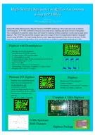
MIMO communication transceiver technologies Mark Rodwell University of California Santa Barbara Rodwelleceucsbedu Acknowledgments 14022022 WMO2 Advances in Circuits
Presentation Embed Code
Download Presentation
Download Presentation The PPT/PDF document "D-band CMOS+InP and CMOS-only" is the property of its rightful owner. Permission is granted to download and print the materials on this website for personal, non-commercial use only, and to display it on your personal computer provided you do not modify the materials and that you retain all copyright notices contained in the materials. By downloading content from our website, you accept the terms of this agreement.
D-band CMOS+InP and CMOS-only: Transcript
Download Rules Of Document
"D-band CMOS+InP and CMOS-only"The content belongs to its owner. You may download and print it for personal use, without modification, and keep all copyright notices. By downloading, you agree to these terms.
Related Documents