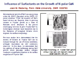
/
Smart  GaN -Based Inverters for Grid-tied Energy Storage Systems Smart  GaN -Based Inverters for Grid-tied Energy Storage Systems

Smart GaN -Based Inverters for Grid-tied Energy Storage Systems - PowerPoint Presentation

blastoracle
blastoracle . @blastoracle
Follow
346 views
Uploaded On 2020-08-28

Smart GaN -Based Inverters for Grid-tied Energy Storage Systems - PPT Presentation

DOEOE Peer Review 09252019 Sandia National Laboratories is a multimission laboratory managed and operated by National Technology and Engineering Solutions of Sandia LLC a wholly owned subsidiary of Honeywell International Inc for the US Department of Energys National Nuclear Secur ID: 809072

gate gan based thermal gan gate thermal based power sbir lbs doe system inverter phase switching mode heat fast

Share:

Link:

Embed:

Download Presentation from below link

Download The PPT/PDF document "Smart GaN -Based Inverters for Grid-tie..." is the property of its rightful owner. Permission is granted to download and print the materials on this web site for personal, non-commercial use only, and to display it on your personal computer provided you do not modify the materials and that you retain all copyright notices contained in the materials. By downloading content from our website, you accept the terms of this agreement.


Presentation Transcript

Slide1

Smart GaN-Based Inverters for Grid-tied Energy Storage Systems

DOE/OE Peer Review, 09/25/2019

Sandia National Laboratories is a

multimission

laboratory managed and operated by National Technology and Engineering Solutions of Sandia, LLC, a wholly owned subsidiary of Honeywell International, Inc., for the U.S. Department of Energy’s National Nuclear Security Administration under contract DE-NA0003525.

1

Innovation City, Power and Energy

Solutions

DOE SBIR Phase IIB

SAND Number: SAND2019-10984 PE

Slide2

Acknowledgement

InnoCit greatly appreciates support of Dr. Imre Gyuk

and Dr. Stan Atcitty through DOE SBIR grant DE-SC0013818.2

Founded in 2014

Tech Transfer Startup

4,000 sq. ft. research facility, 10 acre campus, solar farm, based in Missouri

DOE SBIR Phase I, II, IIB, NSF SBIR Phase I

Costume manufacturing

Slide3

3

System Specifications

GaN

-based

multilevel

inverter

Nominal input voltage: 900V

Output voltage: 3-phase 480VPower rating: 20kW to 200kW

Slide4

4

Specific Objectives

Designing 3U rack-chassis-based enclosures for inverter modulesConduct thermal analysis on the enclosures

Controls and hardware for hot-swap capabilitiesValidate final metrics: efficiency of at least 98.6%, weight < 2.2 lb./kW, volume <0.1 ft3/kW, noise <45

dBaReliability testing including active bypass and hot-swap featuresIEEE 1547,

UL 1741, and 1741-SA testing for islanding and fault

ride-throughUL certification testingRemote control and monitoring backbone structure development

Slide5

Fast-Paced Technology5

Technology / manufacturer

Transphorm

EPC

GaN

systems

GaN

systemsSwitch topologyCascode: GaN JFET + Si MOSFETEnhancement mode FETEnhancement mode FET

Enhancement mode FET

Material

GaN + Si

GaN

GaN

GaN

Part number

TPH3205WS

EPC2034

GS66508T

GS66516T

Voltage

600 V

200 V

650 V

650 V

Current36 A31 A30 A60 ARds-on @ 150 ̊C0.10 Ω0.015 Ω0.050 Ω0.025 ΩCRSS (Reverse transfer)17.5 pF5 pF2 pF4 pFHeatsink PlatenoYesYes

Slide6

Achievements6

First ever floating supply integrated

GaN gate driver + switch (commercialized)First ever modular GaN-based 20-kW inverter (TRL-6)

Slide7

Final System

7

Slide8

Intelligent Inverter

8

Slide9

Commercial Competitiveness9

Features\Manufacturer

InnoCit

Ganverter

(10 units)

Princeton Power

BIGI-250

ABBESSpro-C250

DynaPowerMPS-100

Total Power Rating (S)200-kVA265-kVA200-kVA100-kVACEC Efficiency99%

94.5%

>94%

93.9%

Volume

30-ft

3

(full system + rack)

150-ft

3

41-ft

3

48-ft

3

Weight

540-lbs. (full system + rack)

3500-lbs.

2100-lbs.1545-lbs.Current THD<2% <5%<5%<5%End-user Price per VA$0.085/VA$0.44/VA $0.58/VA$0.52/VA

Slide10

Lessons Learned

Gate driver design is very criticalRequires isolated gate

drivers and isolated

dc-dc power supplies for driving the gateWhen selecting the isolated gate driver and gate power supply, one should ensure that they can withstand the high dv/dt stress due to faster turn ON and OFF

timesWith the fast switching of GaN E-HEMTs

, any parasitic inductances in the gate switching loop will give rise to ringing which leads to losses and EMI

problems - keep the PCB gate-source loop as small as possibleBest switching performance can be achieved with proper selection of gate resistor

Slide11

Lessons Learned

Poor thermal conductivity of GaN semiconductor calls for special attention to thermal designGaN E-HEMTs have tiny packaging compared to

SiC. Therefore, the heat generated within the device has to be dissipated fast and effectively to keep the junction temperature within allowable

limitsAlso, the maximum junction temperature of the GaN E-HEMT selected is low compared to the SiC device

If using a single heat sink for multiple GaN devices, they have to be aligned flat with the surface of heat sinkUsing thermal grease along with thermal tape will provide the best thermal conductivity

Slide12

Contact Information

Mehdi FerdowsiInnoCit, LLCPresident & CEO

ferdowsi@innocit.com

12