PPT-Contrast Properties of Electron Beam Resist
Author : calandra-battersby | Published Date : 2017-06-08
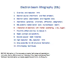
Ahmed Al Balushi Overview Resist materials Sensitivity Contrast Development curves Resist contrast Conclusion QampA Resist Materials Important properties of resist
Presentation Embed Code
Download Presentation
Download Presentation The PPT/PDF document "Contrast Properties of Electron Beam Res..." is the property of its rightful owner. Permission is granted to download and print the materials on this website for personal, non-commercial use only, and to display it on your personal computer provided you do not modify the materials and that you retain all copyright notices contained in the materials. By downloading content from our website, you accept the terms of this agreement.
Contrast Properties of Electron Beam Resist: Transcript
Download Rules Of Document
"Contrast Properties of Electron Beam Resist"The content belongs to its owner. You may download and print it for personal use, without modification, and keep all copyright notices. By downloading, you agree to these terms.
Related Documents