PPT-Nanoscale Optics and Photonics
Author : cheryl-pisano | Published Date : 2018-11-09
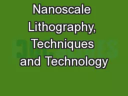
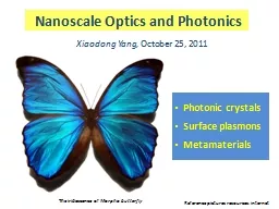
Xiaodong Yang October 25 2011 The iridescence of Morpho butterfly Photonic crystals Surface plasmons Metamaterials Reference pictures resources internet The scale
Presentation Embed Code
Download Presentation
Download Presentation The PPT/PDF document "Nanoscale Optics and Photonics" is the property of its rightful owner. Permission is granted to download and print the materials on this website for personal, non-commercial use only, and to display it on your personal computer provided you do not modify the materials and that you retain all copyright notices contained in the materials. By downloading content from our website, you accept the terms of this agreement.
Nanoscale Optics and Photonics: Transcript
Download Rules Of Document
"Nanoscale Optics and Photonics"The content belongs to its owner. You may download and print it for personal use, without modification, and keep all copyright notices. By downloading, you agree to these terms.
Related Documents