PDF-Fabrication of nm channel length polymer organic thinlm transistors using nanoimprint
Author : debby-jeon | Published Date : 2015-01-14
Austin a and Stephen Y Chou NanoStructure Laboratory Department of Electrical Engineering Princeton University Princeton New Jersey 08540 Received 10 July 2002 accepted
Presentation Embed Code
Download Presentation
Download Presentation The PPT/PDF document "Fabrication of nm channel length polyme..." is the property of its rightful owner. Permission is granted to download and print the materials on this website for personal, non-commercial use only, and to display it on your personal computer provided you do not modify the materials and that you retain all copyright notices contained in the materials. By downloading content from our website, you accept the terms of this agreement.
Fabrication of nm channel length polymer organic thinlm transistors using nanoimprint: Transcript
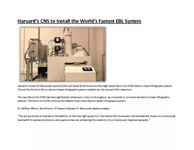
Austin a and Stephen Y Chou NanoStructure Laboratory Department of Electrical Engineering Princeton University Princeton New Jersey 08540 Received 10 July 2002 accepted 9 October 2002 We report on the fabrication of shortchannel polymer organic thin. Concealment, Deception Devices & Enclosures Module 1 . Material & Fabrication course focusing on the use of man made and natural materials to build concealment devices and trojans. Course topics . Nesibe. . Lakhani. EECS 277A. Prof. Richard Nelson. OLED Structure. OLEDs are . light emitting devices that have a thin film of organic compounds as its emissive electroluminescent layer. . Fabrication Methods. Michael Johnston. 4/13/2015. Abstract and Outline. Nanoscale Lithography. . is an ever growing fabrication process due to technology demands. We are continuously striving to increase the number of transistors on a chip to increase performance. The drive for smaller and faster technologies has caused the development of fabrication techniques that allow us to work at the nanoscale feature size. A few lithography techniques will be explored to show how this whole process works. The processes I will cover include Photo, Electron Beam and X-Ray lithography. These forms of lithography share a common process of preparation exposure and development while fabricating wafers.. NANO 101. Introduction to Nanotechnology. 1. 2. Lithography. Photolithography. Electron beam lithography. X-ray lithography. Focused ion beam lithography. “Photoengraving”. Transfer pattern into reactive polymer film (“resist”). Camille Cruz. Chase Thompson. Tyler Nelson. September 26, 2013. Outline. Introduction. Transistors Types. Bipolar Junction Transistors. Field Effect Transistors. Power Transistors. Example. What is a Transistor?. Superhydrophobicity. For the Development of Absorbent for Organic Solvent with High Water Stability. Advantage. Superhydrophobic. porous coordination polymer . (Water contact angle over 150°) . Nano. Imprint Lithography. Lithography. Imprint-To produce (a mark or pattern) on a surface by pressure. .. Nanoscale. Uv. - Method. This was first invented . by Prof. Stephen Chou . and his students in 1995.. Ziam Ghaznavi. CHE 384T Lithography. November 30. th. , 2017. 1. Outline/Agenda. Motivation. Ion – Solid Interactions. Overview of IBL Systems . Future Outlook. 2. Motivation. SEMATECH and the ITRS. Ziam Ghaznavi. CHE 384T Lithography. November 30. th. , 2017. 1. Outline/Agenda. Motivation. Ion – Solid Interactions. Overview of IBL Systems . Future Outlook. 2. Motivation. SEMATECH and the ITRS. Lakhani. EECS 277A. Prof. Richard Nelson. OLED Structure. OLEDs are . light emitting devices that have a thin film of organic compounds as its emissive electroluminescent layer. . Fabrication Methods. Emulsion Polymer Market report published by Value Market Research provides a detailed market analysis comprising of market size, share, value, growth and trends for the period 2018-2025. a brief overview. Montek Singh. Feb . {7. , 12}. , 2018. Transistors as switches. At an abstract level, transistors are merely switches. 3-ported voltage-controlled switch. n-type: conduct when control input is 1. Introduction.. Photon-based lithography: DUV (deep UV), EUV (extreme UV), X-ray. Charged-beam based lithography: electron beam, focused ion beam. Nanofabrication by molding/printing: soft lithography, nanoimprint. Harvard’s Center for Nanoscale Systems(CNS) will install North America’s first High Speed Elionix ELS-HS50 electron beam lithography system. This will be the third Elionix electron beam lithography system installed into the Harvard CNS cleanroom.
Download Document
Here is the link to download the presentation.
"Fabrication of nm channel length polymer organic thinlm transistors using nanoimprint"The content belongs to its owner. You may download and print it for personal use, without modification, and keep all copyright notices. By downloading, you agree to these terms.
Related Documents