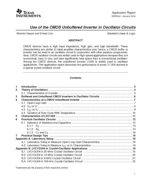
PDF-Use of the CMOS Unbuffered Inverter in Oscillator CircuitsMoshiul Haqu
Author : giovanna-bartolotta | Published Date : 2016-07-04
ic CMOS devices have a high input impedance high gain and high bandwidth Thesecharacteristics are similar to ideal amplifier characteristics and hence a CMOS buffer
Presentation Embed Code
Download Presentation
Download Presentation The PPT/PDF document "Use of the CMOS Unbuffered Inverter in O..." is the property of its rightful owner. Permission is granted to download and print the materials on this website for personal, non-commercial use only, and to display it on your personal computer provided you do not modify the materials and that you retain all copyright notices contained in the materials. By downloading content from our website, you accept the terms of this agreement.
Use of the CMOS Unbuffered Inverter in Oscillator CircuitsMoshiul Haqu: Transcript
ic CMOS devices have a high input impedance high gain and high bandwidth Thesecharacteristics are similar to ideal amplifier characteristics and hence a CMOS buffer orinverter can be used in an o. The HCF4047B consist of a gatable astable multivibrator with logic techniques incorporated to permit positive or negative edgetriggered monostable multivibrator action with retriggering and external counting options Inputs include TRIGGER TRIGGER AS Yousef Shakhsheer. 3/29/2011. 1. VCOs. Two criteria. Generates a periodic output.. Needs self-sustaining oscillation mechanism;. 2. Important Metrics. Frequency. Power. Tunability. (Range and linearity). Tony Affolder. University of Liverpool. LOI Costings. The core costings of the strips for the LOI was done in three parts:. In my spread sheet, I was able to cost:. All components of the stave/petals and off-detector power supplies (LV and HV). 414 – Introduction to VLSI Design. Module #5 –Inverters. Agenda. Inverters. - Static Characteristics. - Switching Characteristics. Announcements. Read Chapters 5, & 7. Inverters. Inverters. Outline. Oscillators. Inverter-Based Oscillator. Introduction of Phase Noise Simulation. LC-Tank Based Oscillator. Laplace Analysis. Circuit Implementation. Quality Factor Analysis. Inverter-Based Oscillator. 8/01/2016. Eaton 1000/1800 True Sine Wave Inverter Aftermarket Installation Instructions. Suggested Inverter Installation Tool List. DC cable kit contents. Instructions for Inverter and DC cable kit Installation for all truck types.. 8/01/2016. Eaton 1000/1800 True Sine Wave Inverter Aftermarket Installation Instructions. Suggested Inverter Installation Tool List. DC cable kit contents. Instructions for Inverter and DC cable kit Installation for all truck types.. Outline. Oscillators. Inverter-Based Oscillator. Introduction of Phase Noise Simulation. LC-Tank Based Oscillator. Laplace Analysis. Circuit Implementation. Quality Factor Analysis. Inverter-Based Oscillator. . James Merlo, Vice President, Reliability Risk Management. Member . Representatives . Committee. February 8, 2017 . Case Study: Blue Cut Fire. On August 16, 2016, the Blue Cut Fire caused thirteen 500 kV line faults and two 287 kV line . Topic 8. - . 1. Topic 8. . Complementary MOS (CMOS) Logic Design. ECE 271. Electronic Circuits I. NJIT ECE 271 Dr, Serhiy Levkov. Topic 8. - . 2. Chapter Goals. Introduce CMOS logic concepts. Explore the voltage transfer characteristics of CMOS inverters. Richard Bates & . Dima. . Maneuski. Contents. Motivation for hybrid CMOS. Assembly. 10/03/16. R. Bates. 2. CMOS designs. Depleted Monolithic Active Pixel Sensor. HR-material (charge collection by drift). Module #4 – CMOS Fabrication. Agenda. CMOS Fabrication. - Yield. - Process Steps for MOS transistors. - Inverter Example. - Design Rules. - Passive Components. - Packaging. Announcements. . (Rs). IC . resistors . have . a . specified . thickness . – . not . under. . the. . control. . of. . the. . circuit. . designer. Eliminate . t . by . absorbing . it. . into . a . new . parameter:. INEL4207. Complex Gate Example. Design a CMOS logic gate for (W/L). p,ref. =5/1 and for (W/L). n,ref. =2/1 that exhibits the function: Y’ = A + BC +BD. By inspection (knowing Y), the NMOS branch of the gate can drawn as the following with the corresponding graph, while considering the longest path for sizing purposes:.
Download Document
Here is the link to download the presentation.
"Use of the CMOS Unbuffered Inverter in Oscillator CircuitsMoshiul Haqu"The content belongs to its owner. You may download and print it for personal use, without modification, and keep all copyright notices. By downloading, you agree to these terms.
Related Documents