PPT-Semiconductor Fundamental and Devices (ELC 302),
Author : jones | Published Date : 2023-12-30
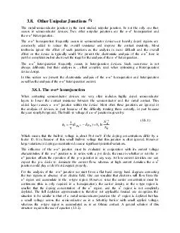
Two Transistor model of SCR What is the two transistor model of SCR Or What is the two transistor analogy of SCR Two transistor analogy of SCR is a method of representing
Presentation Embed Code
Download Presentation
Download Presentation The PPT/PDF document "Semiconductor Fundamental and Devices (E..." is the property of its rightful owner. Permission is granted to download and print the materials on this website for personal, non-commercial use only, and to display it on your personal computer provided you do not modify the materials and that you retain all copyright notices contained in the materials. By downloading content from our website, you accept the terms of this agreement.
Semiconductor Fundamental and Devices (ELC 302),: Transcript
Download Rules Of Document
"Semiconductor Fundamental and Devices (ELC 302),"The content belongs to its owner. You may download and print it for personal use, without modification, and keep all copyright notices. By downloading, you agree to these terms.
Related Documents