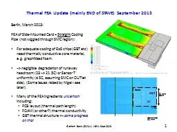
PPT-Procedures and Resources for Composite Fabrication at LBNL

Author : julia | Published Date : 2022-06-11

Composites Group E Anderssen N Hartman LBNL July 2005 E Anderssen LBNL Goal of Talk This is a somewhat heuristic approach to design for fabrication assuming that

Presentation Embed Code

Download Presentation

Download Presentation The PPT/PDF document "Procedures and Resources for Composite F..." is the property of its rightful owner. Permission is granted to download and print the materials on this website for personal, non-commercial use only, and to display it on your personal computer provided you do not modify the materials and that you retain all copyright notices contained in the materials. By downloading content from our website, you accept the terms of this agreement.

Procedures and Resources for Composite Fabrication at LBNL: Transcript


Composites Group E Anderssen N Hartman LBNL July 2005 E Anderssen LBNL Goal of Talk This is a somewhat heuristic approach to design for fabrication assuming that you have a part design in mind and some idea of what the laminate needs to look like ie you know Classical Laminated Plate Theory. Concealment, Deception Devices & Enclosures Module 1 . Material & Fabrication course focusing on the use of man made and natural materials to build concealment devices and trojans. Course topics . 07/15/2010. New progress and homework. 7/15/2010. 1. LBNL-IPHC Phone Conference 07/15/2010. New Progress. MS – JTAG loading problem appears to be solved.. Investigation of Phase-2 internal . mis. -synchronization is still under way.. MICE CC Magnet. Cryostat . Review. Derun. Li. Center for Beam Physics. Lawrence Berkeley National Laboratory. MICE Video Conference. Thursday. , . March 15, 2012. CC . Cryostat Pre-Production Review. Nesibe. . Lakhani. EECS 277A. Prof. Richard Nelson. OLED Structure. OLEDs are . light emitting devices that have a thin film of organic compounds as its emissive electroluminescent layer. . Fabrication Methods. About Us. Plastic Welding and Fabrication, Ltd (PWF) . started in 2003. . L. ike . most other small . businesses PWF started . working out . of a . garage. We have since moved twice . and currently has two buildings in Buda, TX.. 1. Berlin, March 2013:. FEA of Side-Mounted Card + . Straight. Cooling Pipe (not wiggled through SMC region):. For adequate cooling of EoS chips (GBT etc) need thermally conductive core material, e.g. graphitised foam.. Santiranjan Shannigrahi . OUTLINES. :. Polymer-ceramics composites. Basic applications. Current pain. Case study . Conclusions. GRAPH OF MATERIALS PRODUCTION. Source: CES . EduPack. , University of . 32.Passageofparticlesthroughmatter32.PASSAGEOFPARTICLESTHROUGHMATTERRevisedSeptember2013byH.Bichsel(UniversityofWashington),D.E.Groom(LBNL),andS.R.Klein(LBNL).Thisreviewcoverstheinteractionsofphotonsa We've . assembled a team of professional electrical technicians, welders, and fabricators backed by a sales and support staff with over 100 years of combined . experience. . EXPERIENCE YOU CAN TRUST . Lakhani. EECS 277A. Prof. Richard Nelson. OLED Structure. OLEDs are . light emitting devices that have a thin film of organic compounds as its emissive electroluminescent layer. . Fabrication Methods. Oct. __. CONNECT - . Name_____ 6__ Lesson 4 – Prime and Composite Oct. __. CONNECT - . If you can only make 1 pair of factors with the number,. 1 and itself. , then the number is called a ____________. Brought to you by: Jack Link & Aaron Schiller. Date delivered on: Friday the third of May, 2013. ABSTRACT:. Taking a brief look at MicroElectroMechanical Systems (MEMS), we will guide you through the fabrication stages and show you some applications that they are used for. MEMS can be very simple and not move at all to being immensely complex systems with lots of moving elements being controlled by the system. Starting off with some simple facts we will then show the stages of their fabrication. The basic process of manufacturing MEMS starts with deposition of thin films onto their respective material layers. Then the material is patterned by one of many forms of lithography. The final step in creating MEMS is etching the pattern so that the final product will be the desired shape. MEMS can be created at a relatively low cost because they can be produced in high volumes because of bulk fabrication. MEMS are used for microvalves for controlling gas and liquid, switches, sensors, actuators, and much more!. Center for Beam Physics . Lawrence Berkeley National Laboratory. MAP Winter Meeting at SLAC. March 6, 2012. MICE RF System Overview. Hardware. Two RFCC modules: two pairs of four 201-MHz RF cavities with 16 coaxial loop RF couplers and ceramic RF windows (two per cavity) - . New cavity materials . Nb. -Cu composite. New . fabrication methods. Hydroforming. Spinning. Cavity Material-Cost Reduction. Cost of bulk niobium is a major factor for SRF accelerators. especially for low frequency (<650 MHz).

Download Document

Here is the link to download the presentation.
"Procedures and Resources for Composite Fabrication at LBNL"The content belongs to its owner. You may download and print it for personal use, without modification, and keep all copyright notices. By downloading, you agree to these terms.

Related Documents