/
Graham Beck (QMUL) LBNL Sept.2013 Graham Beck (QMUL) LBNL Sept.2013

Graham Beck (QMUL) LBNL Sept.2013 - PowerPoint Presentation

natalia-silvester
natalia-silvester . @natalia-silvester
Follow
415 views
Uploaded On 2016-05-03

Graham Beck (QMUL) LBNL Sept.2013 - PPT Presentation

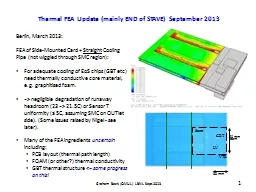
1 Berlin March 2013 FEA of SideMounted Card Straight Cooling Pipe not wiggled through SMC region For adequate cooling of EoS chips GBT etc need thermally conductive core material eg graphitised foam ID: 304353

2013 thermal qmul gbt thermal 2013 gbt qmul foam pipe beck lbnl sept graham cooling fea package stave heat

Share:

Link:

Embed:

Download Presentation from below link

Download Presentation The PPT/PDF document "Graham Beck (QMUL) LBNL Sept.2013" is the property of its rightful owner. Permission is granted to download and print the materials on this web site for personal, non-commercial use only, and to display it on your personal computer provided you do not modify the materials and that you retain all copyright notices contained in the materials. By downloading content from our website, you accept the terms of this agreement.


Presentation Transcript

Slide1

Graham Beck (QMUL) LBNL Sept.2013

1

Berlin, March 2013:FEA of Side-Mounted Card + Straight Cooling Pipe (not wiggled through SMC region):For adequate cooling of EoS chips (GBT etc) need thermally conductive core material, e.g. graphitised foam.=> negligible degradation of runaway headroom (23 => 21.5C) or Sensor T uniformity (≤ 5C, assuming SMC on OUTlet side). (Some issues raised by Nigel - see later).Many of the FEA ingredients uncertain including: PCB layout (thermal path length)FOAM (or other?) thermal conductivityGBT thermal structure <= some progress on this!

Thermal FEA Update (mainly END of STAVE) September 2013

LV

GBT

VTR

foam

30 mm

50 mm

foamSlide2

Graham Beck (QMUL) LBNL Sept.2013

2

Cooling Path & Headroom away from ends of Stave

-33C

-30C

No Sensor heat

SP case

1C bands

Most important contribution to thermal R in pipe region is the fluid film.

Foam – pipe glue joint assembly needs care, to avoid becoming a bottleneck.

Foam conductance is ~ fine! (30W/m-K, good coupling geometry)(Path across stave surface is as important: sensor // facing, through bus tape & glue…)FEA (2011): Runaway Headroom for -30C coolant is 21.5o (23o if allow for P drop). Now aiming to update FEA: power, conductivities, CFRP density, hybrid layout, on-sensor DCDC…(in progress: don’t anticipate more than 2C change).It’s difficult to tell from previous documents what is considered an acceptable headroom: maybe >10o ? We clearly have a lot in hand. (too much? CMS? – next slide)

Thickness L(mm) K(W/mK) L/K (~R) Foam ~1 30 0.03Hysol+BN 0.1 1.6 0.06Ti pipe 0.14 16.4 0.01Fluid Film equiv. 0.1 0.8 0.13 (@ 8000W/m2K)Relative Thermal Path resistance in cylindrical region, close to 2mm dia pipe:Slide3

Graham Beck (QMUL) LBNL Sept.20133COMMENT re Module Cooling geometry.CMS Upgrade Strip modules (Andreas Mussgiller, Oxford Tracker Forum, June 2013)

CO2: -34C Module cooling contacts -27C (Sensor Tmax ~ -20C)(At 3000 fb-1): Runaway when module cooling contacts reach -25Crunaway headroom is 2 degrees (trying to improve on this).ATLAS STAVE strategy - sandwiching the cooling pipes between single-sided modules - allows cooling to be distributed across the sensor …AND …leads naturally to module-pipe contact along the full length of the pipes.(cf. if we suppress the foam around the U-bend we lose ~30% runaway headroom)Slide4

Graham Beck (QMUL) LBNL Sept.2013

4

End of Stave: GBT die temperature. Depends on:GBT Power (estd: 1.8W, more recently: 2.2W “flat out”)GBT Package resistance (unknown at Berlin meeting: assumed 10 C/W).Thermal resistance of PCB (~ layout, vias etc )Foam + CFRP conductance: distance between GBT and pipe. FEA => GBT Temp: +11C (Operation, CO2 at -30C) / +56C (commissioning, above dew-point)…

GBT Package: - High terminal count => Ball Grid Array package. Plastic substrate (cf ceramic).Procurement chain: CERN – IMEC – ASE (Taiwan) <= communications slow!IMEC advice: Typical Thermal resistance die-to-ambient ~ 30 C/W => aim to package with Copper heat spreader and remove heat from TOP.

0.5mm Copper spreader (top) 0.7/0.3mm x 5 x 5mm2 chip

3mm Plastic Substrate20x20 BGA ~0.4mm.

~ 8 layer PCB: 1.6mm FR4

17x17 mm

2

PCB:

Assume 2x17

m

m Cu planes

(! heat spreading near chip).

Thermal

Vias: Not in FEA (needs design): could reduce DT by ×3? In the event, a number of packaged die received at CERN (~ May) had power-ground shorted (most functions test-able after some surgery). Thin (0.25mm) die, integrated capacitors but no clock or Copper heeat slug.One sample obtained by QMUL to investigate thermal resistance to BOTTOM of package. Slide5

Graham Beck (QMUL) LBNL Sept.2013517


0.540.341.14

0.5 dia / 0.8 pitch~ 5.4

Dims measured at QM

Thermal Resistance die-to-bottom measured in “TIMTower”: Slide6

Graham Beck (QMUL) LBNL Sept.201362W, 3W injected into top of chip (calibrated by dT/dZ along upper and lower copper blocks)

~ 10C between ends of blocksCorrected for grease applied to die and BGA (biggest uncertainty)6.5 (±1.5) C/W through package.Verifies heat removal possible through BOTTOM of package -Not enough detail for accurate thermal model when mounted on pcb – but suggests FEA prediction is reasonable (or slightly pessimistic?).Slide7

Graham Beck (QMUL) LBNL Sept.2013

7

SummaryIn absence of the Wiggle”, ~3W EoS(SMC) heat will not seriously degrade runaway performance – at least if the fluid outlet (lower temperature) is on the same side of the stave.GBT chip T: Nothing is quite as effective as wiggling the cooling pipe to pass under the chip. . . . . .but inserting 30W/mK foam into the core can approach it to within ~ 10 degrees . .(+11/+56C) Acceptable? - depends on what is an acceptable chip temperature (assuming model OK!).It would be helpful to understand better:- (trivially) how the hybrids will be placed along Z (symmetrically or not).- dimensions the SMC card – (problem if chips too far from pipe!). - what PCB thermal vias are possible.- packaging / thermal paths of the EoS chips (GBT, GBTLD, GBTLIA, VECSL)- how efficiently the LV conversion can be done.- What are the acceptable T ranges for EoS chips: during operation? during integration? (lifetime/ reliability issue !).Slide8

BACKUP:Plots from Steve McMahon of Current SCT temperature:

Graham Beck (QMUL) LBNL Sept.2013

8Slide9

Graham Beck (QMUL) LBNL Sept.2013

9