PDF-FN3121.9Dual/Quad SPST, CMOS Analog Switches
Author : liane-varnes | Published Date : 2017-01-05
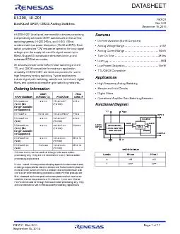
1 TRUT TABE REFERENCEEVE SIFTER ATESxF057ITCSOURCEDRAINOUTPUTOICINPUTVVREFATE Data SheetSeptember 15 2015CAUTION TKese devLces are sensLtLve to eOectrostatLc dLscKarJe
Presentation Embed Code
Download Presentation
Download Presentation The PPT/PDF document "FN3121.9Dual/Quad SPST, CMOS Analog Swit..." is the property of its rightful owner. Permission is granted to download and print the materials on this website for personal, non-commercial use only, and to display it on your personal computer provided you do not modify the materials and that you retain all copyright notices contained in the materials. By downloading content from our website, you accept the terms of this agreement.
FN3121.9Dual/Quad SPST, CMOS Analog Switches: Transcript
Download Rules Of Document
"FN3121.9Dual/Quad SPST, CMOS Analog Switches"The content belongs to its owner. You may download and print it for personal use, without modification, and keep all copyright notices. By downloading, you agree to these terms.
Related Documents