/
MT TUTORIAL Converting Oscillator Phase Noise to Time Jitter by Walt Kester INTRODUCTION MT TUTORIAL Converting Oscillator Phase Noise to Time Jitter by Walt Kester INTRODUCTION

MT TUTORIAL Converting Oscillator Phase Noise to Time Jitter by Walt Kester INTRODUCTION - PDF document

liane-varnes
liane-varnes . @liane-varnes
Follow
633 views
Uploaded On 2014-12-24

MT TUTORIAL Converting Oscillator Phase Noise to Time Jitter by Walt Kester INTRODUCTION - PPT Presentation

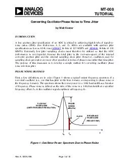
See References 1 2 and 3 ADCs are available with aperture jitter specifications as low as 60fs rms AD9445 14bits 125 MSPS and AD9446 16bits 100 MSPS Extremely low jitter sampling clocks must therefore be utilized so that the ADC performance is n ID: 28974

See References

Share:

Link:

Embed:

Download Presentation from below link

Download Pdf The PPT/PDF document "MT TUTORIAL Converting Oscillator Phase ..." is the property of its rightful owner. Permission is granted to download and print the materials on this web site for personal, non-commercial use only, and to display it on your personal computer provided you do not modify the materials and that you retain all copyright notices contained in the materials. By downloading content from our website, you accept the terms of this agreement.


Presentation Transcript

by Walt Kester A low aperture jitter specification of an ADC is critical to achieving high levels of signal-to-. ADCs are available with aperture jitter specifications as low as 60-fs rms ( MSPS). Extremely low jitter sampling clocks mustperformance is not degraded, because the total jitter is the root-sum-square of the internal sampling clock generation are more often specified in terms of phase noise rather than time jitter. a simple method for converting oscillator phase noise into time jitter. PHASE NOISE DEFINED a typical output frequency spectrum of a PHASENOISE(dBc/Hz) "CLOSE-IN"PHASE NOISE BROADBANDPHASE NOISE 1Hz BW Figure 1: Oscillator Power Spectrum Due to Phase Noise Rev.A, 10/08, WK Page 1 of 10 MT-008 The sampling process is basically a multiplication of the sampling clock and the analog input signal. This is multiplication in the time domain, which is equivalent to convolution in the frequency domain. Therefore, the spectrum of the sampling clock oscillatopure sinewave input signal (see Figure 2). IDEALADC ANALOGINPUT, f DSP fs fofs IDEAL SINEWAVEINPUTSAMPLING CLOCKWITH PHASE NOISE SNRFOR IDEAL ADCWITH N (MEASURED FROM DC TO f/2)CLOSE-INBROADBAND SNR = 20log fff Figure 2: Effect of Sampling Clock "smear" the fundamental signal inthereby reducing the overall spectral resolution. The "broadband" phase noise will cause a tf2log20. Eq. 1 It is customary to characterize an oscillator in terms of its single-sidebain Figure 3, where the phase noise in dBc/Hz isthe frequency axis on a log scale. Note the actual curve is approximated by a number of regions, dB/decade), and x = 1 corresponds to the "flicker" phase noise region (slope = –20 dB/decade). e regions occur progressively closer to the carrier frequency. Page 2 of 10 MT-008 PHASENOISE(dBc/Hz)FREQUENCY OFFSET, f, (LOG SCALE) 1f 1f 2 1f 3 "WHITE" PHASE NOISE"FLICKER" PHASE NOISE CORNER FREQUENCY Figure 3: Oscillator Phase Noise inNote that the phase noise curve is somewhat analof an amplifier. Like amplifiean oscillator. We have seen that oscillators are typically specified in terms of phase noise, but in order to relate phase noise to ADC performance, the phase noise mustr. In order to make the graph relevant to modern ADC applications, the oscillator frequency (sampling frequency) is that the phase noise curve is approximated by a number of individual line segments, and the end points of each segment are defined by data points. 10k 100k1M 10M 100M 1G FREQUENCY OFFSET (Hz) RMS PHASE JITTER (radians) A/10AREA = INTEGRATED PHASE NOISE POWER (dBc)RMS JITTER (seconds) = OSCILLATOR FREQUENCY (100MHz) = 200MHzPHASENOISE(dBc/Hz) INTEGRATE TO2•10A/10 A1 A2 A3 A = 10 log(A1 + A2 + A3 + A4) Figure 4: Calculating Jitter from Phase Noise Page 3 of 10 MT-008 The first step in calculating the equivalent rms jitter is to obtain the integrated phase noise power number of individual areas by two data points. Generally for the integration should be twice the sampling frequency, assuming there is no filtering be input. This approximates the bandwidth of the ADC sampling clock input. some judgment. In theory, it should be as low as possible to get the true rms jitter. In practice, however, the oscillator specifications generally will not be given for offset frequencies less than 10 Hz, or so—however, s in the calculations. A lower frequency of integration of 100 Hz is reasonable in most cases, use either the 1-kHz orsystem, while the broadband noise affects the overall system SNR. Probably the wisest approach is to integrate each area separately as explained below and examine the magnitude of the jitter contribution of each area. The low frequency contributions may be negligible compared to the broadband contribution if a crystal oscillator is used. Other types of oscillators may have significant jitter contributions in the low frequencst be made regarding their importance to the overall The integration of each individual area yields individual power ratios. The individual power ratios are then summed and converted back intoknown, the rms phase jitter in radi 10/A102)radians(JitterPhaseRMSâ‹…=, Eq. 2 10/Af2102)onds(secJitterPhaseRMS. Eq. 3 It should be noted that computer programs and spreadsheets are available online to perform the integration by segments and calculate the rms jitter, thereby greatly simplifying the process Figure 5 shows a sample calculation which assumes only broadband phase noise. The broadband so the jitter number obtained re(expressed as a ratio) is multiplied by the bandwintegrated phase noise of –67 dBc. Note that this multiplication is equivalent to adding the Page 4 of 10 MT-008 – in dBc/Hz. In practice, the lower frequency limit of 0.01 MHz can be dropped from the not affect the final result significantly. A total rms jitter of approximately 1 ps is obtained using Eq. 3. 10k 100k 10M 100M 1G FREQUENCY OFFSET (Hz) = OSCILLATOR FREQUENCY (100MHz) = 200MHzPHASENOISE(dBc/Hz)INTEGRATE TO –150RMS PHASE JITTER (radians) 2•10 = 6.32radiansA/10RMS JITTER (seconds) =RMS PHASE JITTER (radians) A = –150dBc + 10 log –0.01= –150dBc + 83dB = –67dBc = 1ps Crystal oscillators generally offer the lowest possible phase noise and jitter, and some examples are shown for comparison in Figure 6. All the oscillators showfrequency of 20 kHz, and the phase noise therefore represents the white phase noise level. The two Wenzel oscillators are fixed-frequency and represent excellent performance (Reference 9). It is difficult to achieve this level of performance with variable frequencshown by the –150 dBc specification for a relatively high quality generator. Wenzel ULN Series*–174dBc/Hz @ 10kHz+ Wenzel Sprinter Series,–165dBc/Hz @ 10kHz+High Quality Signal Generator –150dBc/Hz @ 10kHz+ Thermal noise floor of resistive source in a matched system @ +25°C= –174dBm/Hz0dBm = 1mW = 632mV p-p into 50* An oscillator with an output of +13dBm (2.82V p-p) into 50with a phase noise of –174dBc/Hz has a noise floor of+13dBm –174dBc = –161dBm, 13dB above the thermal noise floor(Wenzel ULN and Sprinter Series Specifications and Pricing Used with Permission of Wenzel Associates) Figure 6: 100-MHz Oscillator Broadband Phase Noise Floor Comparisons (Wenzel ULN and Sprinter Series Specifications and Pricing used with Permission of Wenzel Page 5 of 10 MT-008 At this point, it should be noted that there is a theoretical limit to the noise floor of an oscillator determined by the thermal noise of a matched source: –174 dBm/Hz at +a noise floor of –174 dBc + 13 dBm = –161 dBm. ThisFigure 7 shows the jitter calculations from the two Wenzel crystal oscillators. In each case, the for the manufacturer's data sheet. Because of the low 1/f corner frequency, the majority of the jitter is due to the "white" phase noise area. The calculated values ely low jitter. For informational purposes, the ributions of each area have been labeled separately. The total jitter is the root-sum-square of the indi 1001k10k100k 1M 10M–120–130–140–150–160–170–180 (–125dBc/Hz, 100Hz) (–150dBc/Hz, 1kHz) (–174dBc/Hz, 10kHz)(–174dBc/Hz, 200MHz) 0.01ps0.002ps0.063ps TOTAL RMS JITTER = 0.064psFREQUENCY OFFSET (Hz)PHASENOISE(dBc/Hz) 1001k10k100k 1M 10M–120–130–140–150–160–170–180 (–120dBc/Hz, 100Hz) (–150dBc/Hz, 1kHz) (–165dBc/Hz, 10kHz)(–165dBc/Hz, 200MHz) 0.02ps0.003ps0.18ps TOTAL RMS JITTER = 0.18psFREQUENCY OFFSET (Hz)PHASENOISE(dBc/Hz)WENZEL STANDARD 100MHz-SC ULTRA LOWNOISE (ULN) CRYSTAL OSCILLATORWENZEL STANDARD 100MHz-SC SPRINTERCRYSTAL OSCILLATOR 100M 100M Figure 7: Jitter Calculations for Low Noise 100-MHz Crystal Oscillators (Phase Noise Data used with PeIn system designs requiring low jitter sampling prohibitive. An alternative solution is ed oscillator to "clean up" a noisy system clock as shown in Figure 8. There are many good references on PLL design (see References 10-13, for example), and we will not pursue that topic further, other than to state that using a narrow bandwidth loop filter in conjunction with a voltage-controlled crystal oscillator (VCXO) typically gives the while at the same time, reducing the overall phanoise floor can be obtained by following the P Page 6 of 10 MT-008 PHASEDETECTOR CHARGEPUMP FILTER BPF ADC SAMPLINGCLOCK NOISYCLOCK fsfsfsfs VCXO DIVIDER ADF4001, OR ADF41xx-SERIES Filter to Condition a "close-in" phase noise is reduced significantly by the action of the PLL. Figure 9: Phase Noise for a Free-Running VCO and a PLL-Connected VCO Page 7 of 10 MT-008 quency synthesis products, including DDS systems, N, and fractional-N PLLs. For example, the ADF4360 family are fully integrated PLLs complete with an internal VCO. With a 10-kHz bandwADF4360-1 -segment approximation and jitter calculations shown in Figure 11. Note that the rms jitter is only 1.57 ps, even with a non-crystal VCO. PHASENOISE(dBc/Hz) Figure 10: Phase Noise for ADF4360-1 2.25-GHz PLL 1001k10k100k1M10M100M1G –80–90–100–110–120–130–140–150 4.5G (–82dBc/Hz, 100Hz)(–77dBc/Hz, 10kHz)(–112dBc/Hz, 100kHz)(–134dBc/Hz, 1MHz)(–146dBc/Hz, 10MHz)(–146dBc/Hz, 4.5GHz)0.28ps0.89ps0.07ps0.03ps0.34ps TOTAL RMS JITTER = 1.57psPHASENOISE(dBc/Hz)FREQUENCY OFFSET (Hz) (–80dBc/Hz, 1kHz) –701.21ps Figure 11: Line Segment Approximation to ADF4360-1, 2.25-GHz PLL Phase Noise Showing Jitter Page 8 of 10 MT-008 heavily on textbooks and application notes to assist in the design ith Analog Devices free downloadable ADIsimPLL design is much easier. To start, choose a circuit by entering the desired output frequency range, ized for phase noise, phase margin, gain, spur levels, lock time, etc., in both the frequency and time domain. The program also performs the rms jitter calculation based on the PLL phase noise, thereby allowing the evaluation of the final PLL output as a sampling clock. Sampling clock jitter can be disastrous to the SNR performance of high performance ADCs. Although the relationship between SNR and jitter is well known, most oscillators are specified in terms of their phase noise. This article has showthe SNR degradation can be easily calculated. d alone crystal oscillators, modern PLLs using jitter performance suitmost demanding requirements. The entire problem of clock distribution has become much more critical because of low jitter requirements. Analog Devices is stribution ICs to serve these needs (www.analog.com/clocks). Page 9 of 10 Page 10 of 10 REFERENCES Brad Brannon, "Aperture Uncertainty and ADC System Performance, Application Note AN-501, Analog Devices, download at http://www.analog.com. Bar-Giora Goldberg, "The Effects of Clock Jitter on Data Conversion Devices," RF Design, August 2002, pp. 26-32, http://www.rfdesign.com. Ulrich L. Rohde, Digital PLL Frequency Synthesizers, Theory and Design, Prentice-Hall, 1983, ISBN 0-13-214239-2, all of Chapter 2 and pp. 411-418 for computer analysis. Joseph V. Adler, "Clock-Source Jitter: A Clear Understanding Aids Oscillator Selection," EDN, February 18, 1999, pp. 79-86, http://www.ednmag.com. Neil Roberts, "Phase Noise and Jitter – A Primer for Digital Designers," EEdesign, July 14, 2003, http://www.eedesign.com. Boris Drakhlis, "Calculate Oscillator Jitter by using Phase-Noise Analysis Part 1," Microwaves and RFJanuary 2001, p. 82, http://www.mwrf.com. Boris Drakhlis, "Calculate Oscillator Jitter by using Phase-Noise Analysis Part 2," Microwaves and RFFebruary 2001, p. 109, http://www.mwrf.com. Raltron Electronics Corporation, 10651 Northwest 19th Street, Miami, Florida 33172, Tel: (305) 593-6033, http://www.raltron.com . (see "Convert SSB Phase Noise to Jitter" under "Engineering Design Wenzel Associates, Inc., 2215 Kramer Lane, Austin, Texas 78758, Tel: (512) 835-2038, http://www.wenzel.com (see "Allan Variance from Phase Noise" under "Spreadsheets"). 10.Mike Curtin and Paul O'Brien, "Phase-Locked Loops for High-Frequency Receivers and Transmitters, Part 1 Analog Dialogue 33-3, 1999, http://www.analog.com. 11.Mike Curtin and Paul O'Brien, "Phase-Locked Loops for High-Frequency Receivers and Transmitters, Part 2 Analog Dialogue 33-5, 1999, http://www.analog.com. 12.Phase-Locked Loops: Theory, Design and Applications, Fourth Edition, McGraw-Hill, 1999, ISBN 0071349030. 13.F. M. Gardner, Phaselock Techniques, Second Edition, John Wiley, 1979, ISBN 0471042943. Copyright 2009, Analog Devices, Inc. All rights reserved. Analog Devices assumes no responsibility for customer product design or the use or application of customers’ products or for any infringements of patents or rights of others which may result from Analog Devices assistance. All trademarks and logos are property of their respective holders. Information furnished by Analog Devices applications and development tools engineers is believed to be accurate and reliable, however no responsibility is assumed by Analog Devices regarding technical accuracy and topicality of the content provided in Analog Devices Tutorials.